
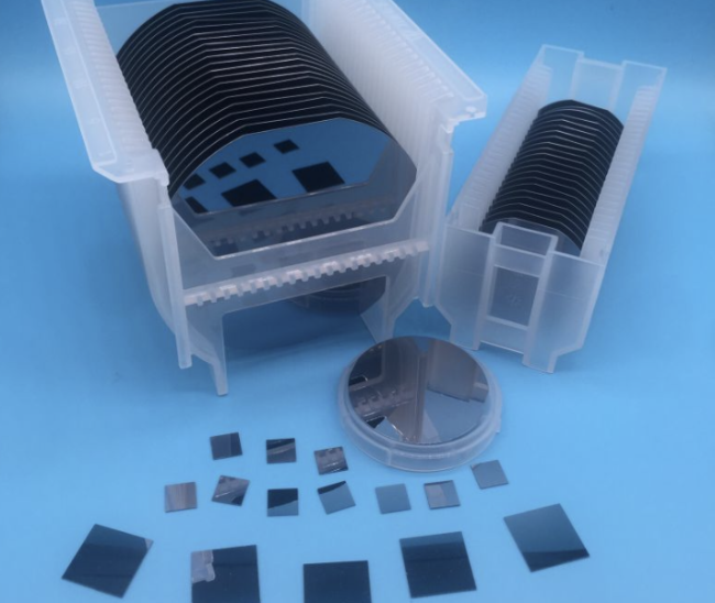
VGF 2 Inch 4Inch N / P Type GaAs Wafer Semiconductor Substrate For Epitaxial Growth
VGF 2 Inch 4Inch N Type P Type GaAs Wafer Semiconductor Substrate For Epitaxial Growth
VGF 2inch 4inch 6inch n-type prime grade GaAs wafer for epitaxial growth
Gallium arsenide can be made into semi-insulating high-resistance materials with resistivity more than 3 orders of magnitude higher than silicon and germanium, which are used to make integrated circuit substrates, infrared detectors, gamma photon detectors, etc. Because its electron mobility is 5 to 6 times greater than that of silicon, it has important applications in the manufacture of microwave devices and high-speed digital circuits. Gallium arsenide made of gallium arsenide can be made into semi-insulating high-resistance materials with resistivity of more than 3 orders of magnitude higher than silicon and germanium, which are used to make integrated circuit substrates and infrared detectors.
1. Application of gallium arsenide in optoelectronics
2. Application of gallium arsenide in microelectronics
3. Application of gallium arsenide in communication
4. Application of gallium arsenide in microwave
5. Application of gallium arsenide in solar cells
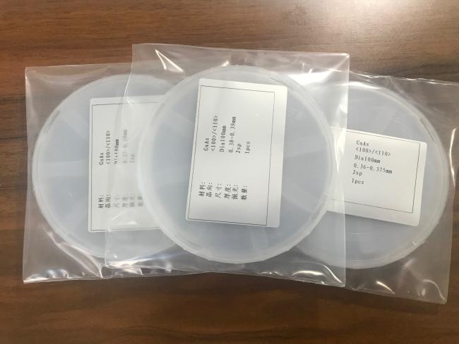
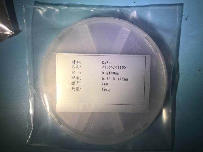
GaAs Wafers Specification
| Type/Dopant | Semi-Insulated | P-Type/Zn | N-Type/Si | N-Type/Si |
| Application | Micro Eletronic | LED | Laser Diode | |
| Growth Method | VGF | |||
| Diameter | 2", 3", 4", 6" | |||
| Orientation | (100)±0.5° | |||
| Thickness (µm) | 350-625um±25um | |||
| OF/IF | US EJ or Notch | |||
| Carrier Concentration | - | (0.5-5)*1019 | (0.4-4)*1018 | (0.4-0.25)*1018 |
| Resistivity (ohm-cm) | >107 | (1.2-9.9)*10-3 | (1.2-9.9)*10-3 | (1.2-9.9)*10-3 |
| Mobility (cm2/V.S.) | >4000 | 50-120 | >1000 | >1500 |
| Etch Pitch Density (/cm2) | <5000 | <5000 | <5000 | <500 |
| TTV [P/P] (µm) | <5 | |||
| TTV [P/E] (µm) | <10 | |||
| Warp (µm) | <10 | |||
| Surface Finished | P/P, P/E, E/E | |||
Gallium arsenide is the most important and widely used semiconductor material in compound semiconductors, and it is also the most mature and the largest compound semiconductor material in production at present.
Gallium arsenide devices that have been used are:
- Microwave diode, Gunn diode, varactor diode, etc.
- Microwave transistors: field effect transistor (FET), high electron mobility transistor (HEMT), heterojunction bipolar transistor (HBT), etc.
- Integrated circuit: microwave monolithic integrated circuit (MMIC), ultra-high speed integrated circuit (VHSIC), etc.
- Hall components, etc.
- Infrared light-emitting diode (IR LED); Visible light-emitting diode (LED, used as substrate);
- Laser diode (LD);
- Light detector;
- High-efficiency solar cell;
Get in Touch
Have questions about our products or want to discuss a custom order? Our team is ready to help you.