
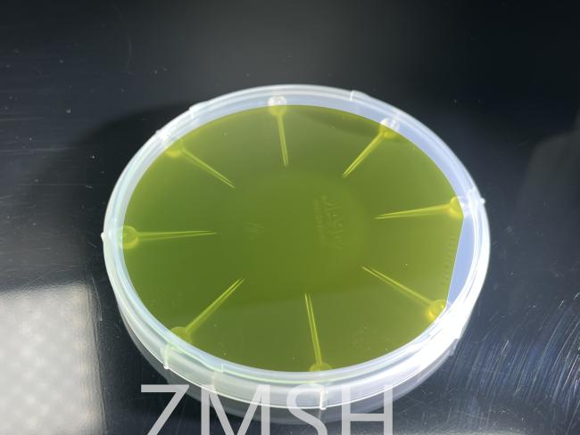
4H N Type Semi Type SiC Wafer 4inch DSP Production Research Dummy Grade Customization
4H N Type Semi Type SiC Wafer 4inch DSP Production Research Dummy Grade Customization
Product Description:
Silicon carbide wafer is mainly used in the production of Schottky diode, metal oxide semiconductor field effect transistors, junction field effect transistors, bipolar junction transistors, thyristors, turn-off thyristors, and insulated gate bipolar transistors. Silicon Carbide Wafer features high/low resistivity, ensuring that it delivers the performance you need, no matter your application's requirements. Whether you're working with high-power electronics or low-power sensors, our wafer is up to the task. So if you're looking for a top-quality Silicon Carbide Wafer that delivers exceptional performance and reliability, look no further than our product. We guarantee that you won't be disappointed with its quality or performance.
| Grade | Zero MPDGrade | Production Grade | Dummy Grade | |
| Diameter | 100.0 mm +/- 0.5 mm | |||
| Thickness | 4H-N | 350 um +/- 20 um | 350 um +/- 25 um | |
| 4H-SI | 500 um +/- 20 um | 500 um +/- 25 um | ||
| Wafer Orientation | On axis: <0001> +/- 0.5 deg for 4H-SI | |||
| Off axis: 4.0 deg toward <11-20> +/-0.5 deg for 4H-N | ||||
| Electrical Resistivity | 4H-N | 0.015~0.025 | 0.015~0.028 | |
| (Ohm-cm) | 4H-SI | >1E9 | >1E5 | |
| Primary Flat Orientation | {10-10} +/- 5.0 deg | |||
| Primary Flat Length | 32.5 mm +/- 2.0 mm | |||
| Secondary Flat Length | 18.0 mm +/- 2.0 mm | |||
| Secondary Flat Orientation | Silicon face up: 90 deg CW from Primary flat +/- 5.0 deg | |||
| Edge exclusion | 3 mm | |||
| LTV/TTV /Bow /Warp | 3um /5um /15um /30um | 10um /15um /25um /40um | ||
| Surface Roughness | Polish Ra < 1 nm on the C face | |||
| CMP Ra < 0.2 nm | Ra < 0.5 nm | |||
| Cracks inspected by high intensity light | None | None | 1 allowed, 2 mm | |
| Hex Plates inspected by high intensity light | Cumulative area ≤0.05% | Cumulative area ≤0.1 % | ||
| Polytype Areas inspected by high intensity light | None | None | Cumulative area≤3% | |
| Scratches inspected by high intensity light | None | None | Cumulative length≤1x wafer diameter | |
| Edge chipping | None | None | 5 allowed, ≤1 mm each | |
| Surface Contamination as inspected by high intensity light | None | |||
Character:
1. Strong High-Temperature Stability: Silicon carbide wafers exhibit extremely high thermal conductivity and chemical inertness, allowing them to maintain stability in high-temperature environments without easily experiencing thermal expansion and deformation.
2. High Mechanical Strength: Silicon carbide wafers have high rigidity and hardness, enabling them to withstand high stresses and heavy loads.
3. Excellent Electrical Properties: Silicon carbide wafers have superior electrical properties compared to silicon materials, with high electrical conductivity and electron mobility.
4. Outstanding Optical Performance: Silicon carbide wafers possess good transparency and strong radiation resistance.
Silicon carbide single crystal growth:

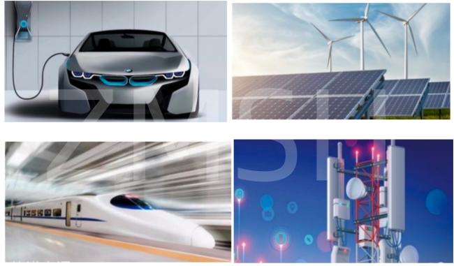
1. Inverters, DC-DC Converters, and Onboard Chargers for Electric Vehicles: These applications require a large number of power modules. Compared to silicon-based solutions, silicon carbide devices bring about a significant increase in driving range and reduction in charging time for electric vehicles.
2. Silicon Carbide Power Devices for Renewable Energy Applications: Silicon carbide power devices used in inverters for solar and wind energy applications enhance energy utilization, providing more efficient solutions for carbon peaking and carbon neutrality.
3. High-Voltage Applications like High-Speed Rail, Metro Systems, and Power Grids: Systems in these fields demand high voltage tolerance, safety, and operational efficiency. Power devices based on silicon carbide epitaxy are the optimal choice for the aforementioned applications.
4. High-Power RF Devices for 5G Communication: These devices for the 5G communication sector require substrates with high thermal conductivity and insulation properties. This facilitates the realization of superior GaN epitaxial structures.
FAQ:
Q: What is the difference between 4H-SiC and SiC?
A: 4H-Silicon Carbide (4H-SiC) stands out as a superior polytype of SiC due to its wide bandgap, excellent thermal stability, and remarkable electrical and mechanical characteristics.
Q: When should SiC be used?
A: If you want to quote someone or something in your work, and you notice the source material contains a spelling or grammatical error, you use sic to denote the error by placing it right after the mistake.
Q: Why 4H SiC?
A: 4H-SiC is preferred over 6H-SiC for most electronics applications because it has a higher and more isotropic electron mobility than 6H-


Get in Touch
Have questions about our products or want to discuss a custom order? Our team is ready to help you.