
6 Layers HDI PCB Board FR4 TG170 2u" Immersion Gold With Half Holes
6 Layers HDI PCB Circuit Board Made of FR4 TG 170 in 2u" Immersion Gold with Half Holes
Abis Circuits Co., Ltd is a professional PCB manufacturer which was established on Oct, 2006 and focus on double side, Multilayer and HDI pcb mass production.
We have two factories together , the factory in Shenzhen is specialized in small and middle volume orders and the factory in Huizhou is for big volume and HDI.
What is a HDI PCB?
IPC-2226 defines HDI as a printed circuit board with a higher wiring density per unit area than conventional printed circuit boards (PCB). They have finer lines and spaces ≤ 100 µm / 0.10mm, smaller vias (<150 µm) and capture pads <400 µm / 0.40mm, and higher connection pad density (>20 pads/cm2) than employed in conventional PCB technology.
Product Details:
|
Number of layers |
4 – 22 layers standard, 30 layers advanced |
|
Technology highlights |
Multilayer boards with a higher connection pad density than standard boards, with finer lines/spaces, smaller via holes and capture pads allowing microvias to only penetrate select layers and also be placed in surface pads. |
|
HDI builds |
1+N+1, 2+N+2, 3+N+3,4+N+4, any layer in R&D |
|
Materials |
FR4 standard, FR4 high performance, Halogen free FR4, Rogers |
|
Copper weights (finished) |
18μm – 70μm |
|
Minimum track and gap |
0.075mm / 0.075mm |
|
PCB thickness |
0.40mm – 3.20mm |
|
Maxmimum dimensions |
610mm x 450mm; dependant upon laser drilling machine |
|
Surface finishes available |
OSP, ENIG, Immersion tin, Immersion silver, Electrolytic gold, Gold fingers |
|
Minimum mechanical drill |
0.15mm |
|
Minimum laser drill |
0.10mm standard, 0.075mm advanced |
Capacity:
ELECTRICAL TEST
|
E-testing |
100% |
|
QFP Pitch |
16mil (0.40mm) |
|
BGA Pitch |
16mil (0.40mm) |
|
Connector Pitch |
16mil (0.40mm) |
OTHER OPTIONS
|
AOI |
All Multilayer |
|
Impedance Control |
± 10% |
|
Solderability Testing |
As standard |
|
Ionic Contamination |
On Request |
SOLDER MASK
|
Via Plugging (100% Fill) |
–20% |
|
Via Size |
≤0.50mm |
|
Registration |
0.025mm |
|
Solder Dam Width |
Min. 0.15mm |
|
Thickness Over Trace (Surface) |
Min. 10µm |
|
Solder Mask Pad Size |
Min. 15µm |
Lead time:
|
Board Type |
Manufacturing Lead Time |
|
Single Sided |
5 – 20 Days dependant on volume |
|
PTH |
7 – 25 Days dependant on volume |
|
Multilayer |
15 – 30 Days dependant on volume & Technology |
·
|
Air Freight Lead Time – 4 Days |
|
Sea Freight Lead Time – 30 Days |
|
All Far East lead times are subject to customs clearance |
|
Premium International shipments can be arranged by DHL, Fedex, UPS or TNT at extra cost |
Our mission:
PCBs for demanding customers, on time with zero defects, produced sustainably at the lowest total cost. Manufacturing many different types of PCBs in smaller series (High-mix, Low-volume) involves constantly adjusting, adapting and problem solving.
Our responsibility:
We know that the PCB is a critical key component for our customers. And we know for sure that anything can happen during the complex production process involved – and it often does. In our world, taking full responsibility means a lot of things, including a responsible and sustainable approach in everything we do – socially, environmentally and ethically. When a problem occurs, we try as hard as we can to understand the problem and find a solution. Our mindset is that we own the problem and don’t leave until we have cleared it up.
FAQ:
Q1:What's your Aluminum board Thermal Conductivity?
A: Normally 0.8-3W/m.K. If you have special demands please feel free contact us
Q2:Is my PCB file safe if I send it to you for manufacturing?
A: We respect customer's design authority and will never manufacture PCB for someone else without your permission. NDA is acceptable.
Q3:What is your testing policy and how you control the quality?
A: For sample, usually tested by flying probe; for PCB Volume over 3 square meters, usually tested by fixture, this will be more faster. Due to there's many steps to PCB production, we usually do inspection after every step.
Q4: What's your shipping way ?
A: 1. We have our own forwarder to ship goods by DHL, UPS, FEDEX, TNT,EMS.
2. If you have your own forwarder, we can cooperate with them.
Q5: What is your certificate?
A: ISO9001:2008, ISO14001: 2004, UL, SGS,RoHS report.
Q6: What files should we offer?
A: If only need PCB, please provide Gerber File and manufacturing specifications; If need PCBA,Please provide Gerber File, Manufacturing specification, BOM list and Pick & Place/XY file.
Q7: Can I get a sample?
A: Yes, It's reasonable to get a sample to test our quality at first.
Q8: Does ABIS CIRCUITS bevel gold fingers?
A: Yes. A standard 45-degree bevel, also bevel at 15 or 30 degrees upon request. For multi-layer board, please ensure there is adequate back set for the bevels.
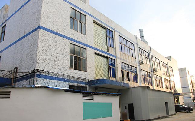
Factory View:


Get in Touch
Have questions about our products or want to discuss a custom order? Our team is ready to help you.