
94v0 1oz Enig Hdi Pcb Board 4layer Oem Fabricating
1OZ ENIG Multilayer 4Layer OEM Fabricating HDI PCB Board
HDI PCB Board Introduction
The High-Density Interconnect (HDI) Printed Circuit Board is HDI PCB Board. There is little space between the PCB components, making the board space smaller, at the same time the board functionally isn’t affected. That is, a PCB with about 120 – 160 pins per square inch is an HDI PCB. All of the other electronic components are mounted on the printed circuit boards(PCBs),which are the foundation.
PCB CAPABILITIES
| FACTORY CAPABILITIES | |||
| No. | Items | 2020 | |
| 1 | HDI Capabilities | HDI ELIC(5+2+5) | |
| 2 | Max layer count | 46L | |
| 3 | Board Thickness | Core thickness 0.05mm-1.5mm ,Fineshed board thickness 0.3-3.5mm | |
| 4 | Min.Hole Size | Laser 0.05mm | |
| Mechnical 0.15mm | |||
| 5 | Min Line Width/Space | 0.030mm/0.030mm | |
| 6 | Copper Thickness | 1/3oz-6oz | |
| 7 | Size Max Panel size | 700x610mm | |
| 8 | Registration Accuracy | +/-0.05mm | |
| 9 | Routing Accuracy | +/-0.05mm | |
| 10 | Min.BGA PAD | 0.125mm | |
| 11 | Max Aspect Ratio | 10:01 | |
| 12 | Bow and Twist | 0.50% | |
| 13 | Impedance Control Tolerance | +/-5% | |
| 14 | Daily output | 4,000m2 (Max capacity of equipment) | |
| 15 | Surface Finishing | HASL Lead Free /ENEPING /ENIG /HASL /FINGER GOLD/IMMERSION TIN/SELECTIVE THICK GOLD | |
| 16 | Raw Material | FR-4/Normal Tg/High Tg/Low Dk/HF FR4/PTEE/PI | |
| PCBA Capability | |||
| Material Type | Item | Min | Max |
| PCB | Dimension (length,width,height.mm) | 50*40*0.38 | 600*400*4.2 |
| Components | Chip&IC | 1005 | 55mm |
| BGA Pitch | 0.3mm | - | |
| QFP Pitch | 0.3mm | - | |
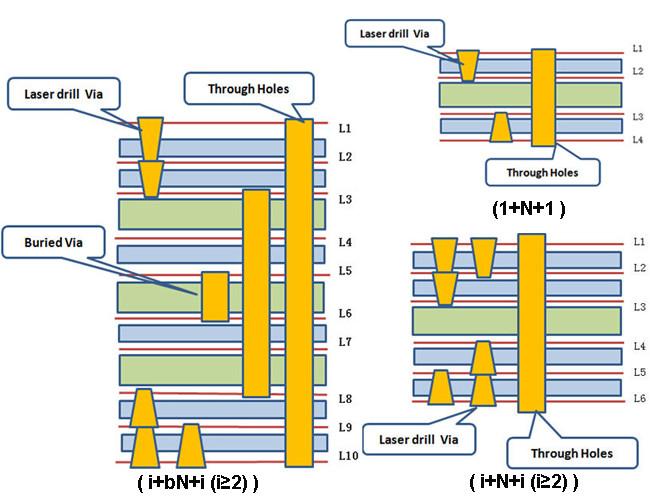
The types of HDI PCB
1.through vias from surface to surface,
2.with buried vias and through vias,
3.two or more HDI layer with through vias,
4.passive substrate with no electrical connection,
5.coreless construction using layer pairs
6.alternate constructions of coreless constructions using layer pairs.
Work flow for HDI
Board Cut - Inner Wet film -DES - AOI - Brown Oxido - Outer Layer Press - Out Layer Lamination - X-RAY & Rounting - Copper reduce & brown oxide - Laser Drilling - Drilling - Desmear PTH - Panel plating - Outer Layer dry film - Etching - AOI- Impedance Testing - S/M Pluged hole - Solder Mask - Component Mark - Impedance testing - Immersion Gold -V-cut - Routing - Electrical Test - FQC - FQA -Package -Shipment


Similar products
Delivery Time
| Product Type | Qty | Normal lead time | Quick-turn lead time |
| SMT+DIP | 1-50 | 1WD-2WD | 8H |
| SMT+DIP | 51-200 | 2WD-3WD | 1.5WD |
| SMT+DIP | 201-2000 | 3WD-4WD | 2WD |
| SMT+DIP | ≥2001 | 4WD-5WD | 3WD |
| PCBA(2-4Layer) | 1-50 | 2.5WD-3.5WD | 1WD |
| PCBA(2-4Layer) | 51-2000 | 5WD-6WD | 2.5WD |
| PCBA(2-4Layer) | ≥2001 | ≥7WD | 5WD |
| PCBA(6-10Layer) | 1-50 | 3WD-4WD | 2.5WD |
| PCBA(6-10Layer) | 51-2000 | 7WD-8WD | 6WD |
| PCBA(10-HDILayer) | 1-50 | 7WD-9WD | 5WD |
| PCBA(10-HDILayer) | 51-2000 | 9WD-11WD | 7WD |
HDI PCB Board Application Field
Our products are widely used in communication equipment, industrial control, consumer electronics, medical equipment, aerospace, light-emitting diode lighting, automotive electronics etc.

Workshop


Common packaging
1.PCB: Vacuum packaging with carton box
2.PCBA: ESD packaging with carton box


Company information
We have profuse experience in manufacturing PCB,owned experienced technical R & D technology team, young and professional sales and customer service team, experienced and professional procurement team and assembly testing team, which make sure the products quality of the pass rate, on-time delivery rate of customer orders.
Our services include: circuit board design and layout, 2-46 layers PCB manufacturing, professional FPC production, electronic components purchasing, SMT professional processing, Soldering and Assembly, especially sample and small bulk orders. we have the advantages of a quick quote, fast production, fast delivery.

Get in Touch
Have questions about our products or want to discuss a custom order? Our team is ready to help you.