
Multilayer FR4 HDI PCB Board 1.6mm 4 Layer Double Sided Pcb Soldering
Multilayer FR4 HDI PCB Board 1.6mm 4 Layer Double Sided Pcb Soldering
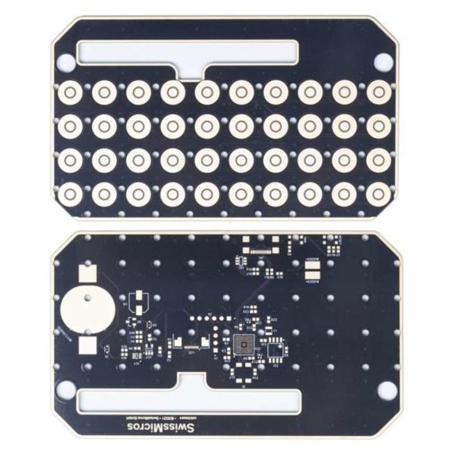
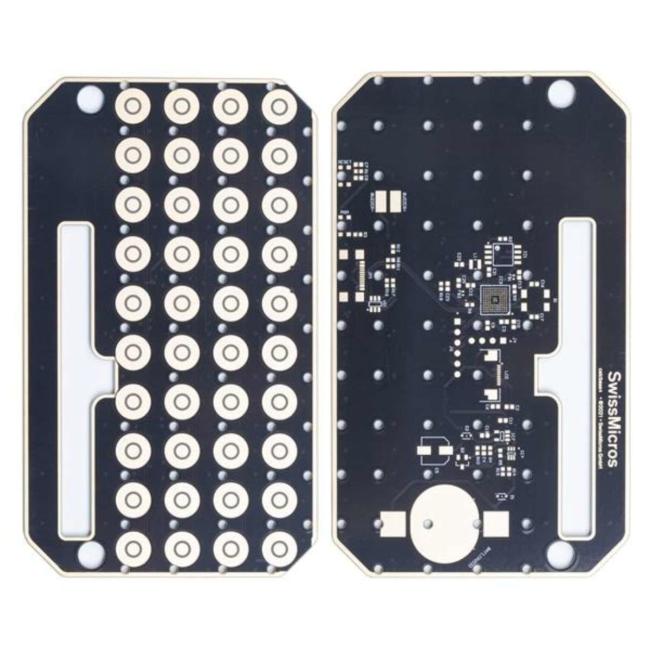
HDI PCB Board HDI Circuit Boards Black PCB Board Multilayer PCB Board PCB Manufacturing Service FR4 PCB board
4L 1+N+1 HDI Boards
What’s HDI PCB? High-density interconnect (HDI) PCBs are characterized by finer lines, closer spaces, and more dense wiring, which allow for a faster connection while reducing the size and bulk of a project. These boards also feature blind and buried vias, laser ablated microvias, sequential lamination, and via in-pads.
A HDI board can house the functionality of the previous boards used. MADPCB is an HDI PCB manufacturer and provider in Shenzhen, China supports HDI PCB prototype and mass production with less expensive price and quick-turn lead time. Customers from a variety of industries we serve have a common that have high expectations in quality, reliability and on-time delivery in HDI PCB production. Our quality is not afterthought, but built into each process from front-end to fabrication and shipping.
| PCB Layer | 4L | PCB material | FR4 TG170 |
| Copper thickness | 1/1/1/1OZ | PCB thickness | 1.6MM |
| Min. hole size | 0.15mm | Min.PCB track/gap: | 4/4mil |
| PCB solder mask | Black | PCB silkscreen | White |
| PCB surface finished | Immersion Gold | PCB outline | Routing/V-CUT/Punching |
| Application | communications | ||
| Special requirement: | HDI Buried vias and blind vias, one step stack up /impedance control | ||
FAQ:
Q1:Could you provide PCB Assembly services and components sourcing?
A: Yes, we could also provide components sourcing and PCB Assembly services as well as box build if request.
Q2:Which countries have you worked with?
A:USA, Canada, Italy, Germany, UK, Spain, France, Russia, Iran, Turkey, Czech Republic,Austria, Australia, Brazil, Japan, India etc.
Q3:Are my PCB files safe when I submit them to you for manufacturing?
A: We respect customer's copyright and will never manufacture PCB for someone else with your files unless we receive written permission from your side, nor we'll share these files with any other 3rd parties. And we could sign NDA with client if necessary.
Q4:If we have no PCB file/Gerber file, only have the PCB sample,can you produce it for me?
A: Yes,we could help you to clone the PCB. Just send the sample PCB to us, we could clone the PCB design and work out it.
Q5:What is your standard lead time for PCB?
A: Sample/prototype(less than 3sqm):
1-2 Layers: 3 to 5working days (fastest 24hours for quick turn services)
4-8 Layers: 7~12 working days (fastest 48hours for quick turn services)
Mass production (less than 200sqm):
1-2 Layers:7 to 12 working days
4-8 Layers:10 to 15 working days
Get in Touch
Have questions about our products or want to discuss a custom order? Our team is ready to help you.