
PCBA Electronics LCD TV 2 Layers PCB HASL ISO14001
2 Layers Pcb Custom Cheap Small Spacing Circuit Board Fr4 Pcb Board PCBA Electronics Circuit Board Design Service
Dear buyer,
Thank you so much for scanning our circuit boards.
As is known, PCB is a customized product, so the unit price is not real, details please contact me and a quotation will be offered.Please send us PCB files in Gerber files, ".pcbdoc", ".lay", ".lay6" or ".brd" .
Would like to know more about the product? Send us an inquiry!
Pls feel free to send us Gerber file for latest price!
|
PCB Bare Board Processing Capacity
|
|
|
|
|
|
Base Material
|
Normal Tg FR4, High Tg FR4, PTFE, Rogers, Low Dk/Df etc.
|
|
|
|
|
Solder Mask Color
|
Green, Red, Blue, White, Yellow, Purple, Black
|
|
|
|
|
Legend Color
|
white, yellow, black, red
|
|
|
|
|
Surface treatment type
|
ENIG, Immersion tin, HAF, HAF LF, OSP, flash gold, gold finger, sterling silver
|
|
|
|
|
Max. layer-up(L)
|
50
|
|
|
|
|
Max. unit size (mm)
|
620*813 (24"*32")
|
|
|
|
|
Max. working panel size (mm)
|
620*900 (24"x35.4")
|
|
|
|
|
Max. board thickness (mm)
|
12
|
|
|
|
|
Min. board thickness(mm)
|
0.3
|
|
|
|
|
Board thickness tolerance (mm)
|
T<1.0mm: +/-0.1mm; T≥1.0mm: +/-10%
|
|
|
|
|
Registration tolerance (mm)
|
+/-0.10
|
|
|
|
|
Min. mechanical drilling hole diameter (mm)
|
0.15
|
|
|
|
|
Min. laser drilling hole diameter(mm)
|
0.075
|
|
|
|
|
Max. aspect(through hole)
|
15:1
|
|
|
|
|
Max. aspect(micro-via)
|
1.3:1
|
|
|
|
|
Min. hole edge to copper space(mm)
|
L≤10, 0.15;L=12-22,0.175;L=24-34, 0.2;L=36-44, 0.25;L>44, 0.3
|
|
|
|
|
Min. innerlay clearance(mm)
|
0.15
|
|
|
|
|
Min. hole edge to hole edge space(mm)
|
0.28
|
|
|
|
|
Min. hole edge to profile line space(mm)
|
0.2
|
|
|
|
|
Min. innerlay copper to profile line space (mm)
|
0.2
|
|
|
|
|
Registration tolerace between holes (mm)
|
±0.05
|
|
|
|
|
Max. finished copper thickness(um)
|
Outer Layer: 420 (12oz) Inner Layer: 210 (6oz)
|
|
|
|
|
Min. trace width (mm)
|
0.075 (3mil)
|
|
|
|
|
Min. trace space (mm)
|
0.075 (3mil)
|
|
|
|
|
Solder mask thickness (um)
|
line corner : >8 (0.3mil) upon copper: >10 (0.4mil)
|
|
|
|
|
BGA pad (mm)
|
≥0.25 (HAL or HAL Free:0.35)
|
|
|
|
|
V-CUT blade position tolerance (mm)
|
+/-0.10
|
|
|
|
|
Impedence tolerance (%)
|
+/-5%
|
|
|
|
|
Min. legend width (mm)
|
0.1 |
|||
|
Fire flame calss
|
94v0
|
|
|
|
|
PCBA Processing Capacity
|
|
|
|
|
|
Processing Service
|
One Stop PCB Assembly service, include components&plastic mold sourcing,SMT&DIP assembly and enclosure installation service.
|
|
|
|
|
Components Package
|
Smallest with 01005, various chips package as QFN,BGA,SSOP,PLCC,LGA..
|
|
|
|
|
Testing
|
100% Function Testing before shipment
|
|||
|
MOQ
|
No MOQ(1PCS)
|
|
|
|
|
Factory Certificate
|
ISO9001:2017;ISO13485;ISO16949
|
|||

Q1:What are the main products of your PCBA service?
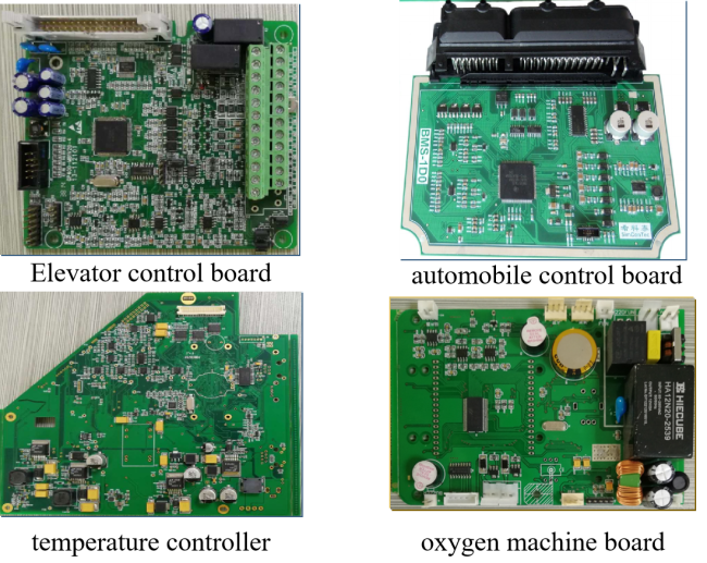
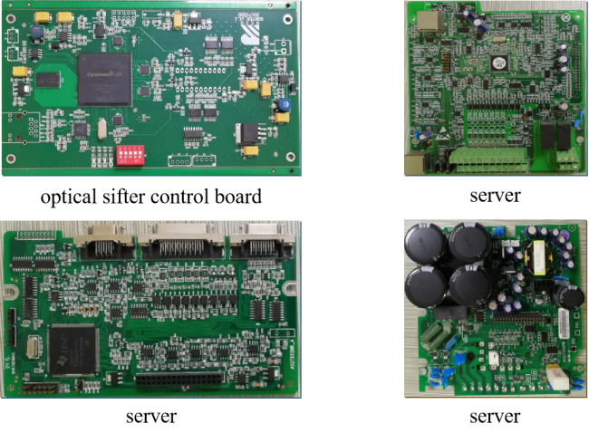
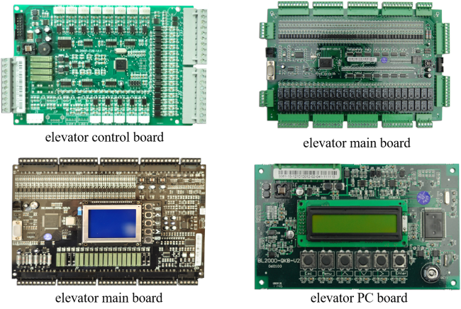
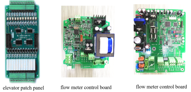
A1:Automotive, medical devices, computer, digital, telecommunication, elevator, airplane, home appliance etc.
Q2:What is your Minimum Order Quantity (MOQ)?
A2:As for MOQ, we have no request about it. Even 1 Pcs is ok for us.
Q3:What service do you have?
A3:We can provide OEM ODM EMS service. If your team already have design files,we can help you do PCB fabrication, PCB/Component sourcing, PCB assembly,PCBA programming and testing,mold injection, final product assembly and testing etc.EMS(Electronic Manufacturing Service),Printed circuit board assembly
Q4: How can we get the PCB/PCBA quotation?
A4: For PCB, pls provide the PCB Gerber files and basic PCB infos(Material type, board thickness, copper thickness,soldermask,silkscreen,surface finish etc.)
A4: For PCBA,Pls provide the PCB Gerber files and BOM list.
Get in Touch
Have questions about our products or want to discuss a custom order? Our team is ready to help you.