6-16 Layer High-Frequency PCB Assembly for IoT | 0.2mm Hole Size, 4-6mil Trace Width, -40°C to 85°C Operating Range
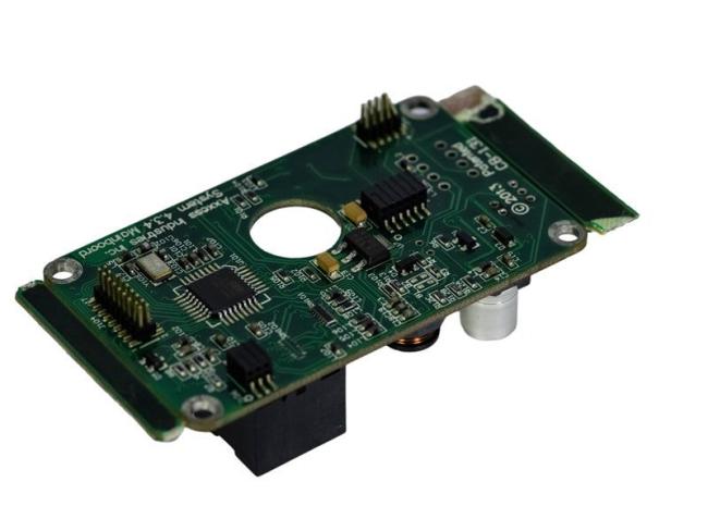
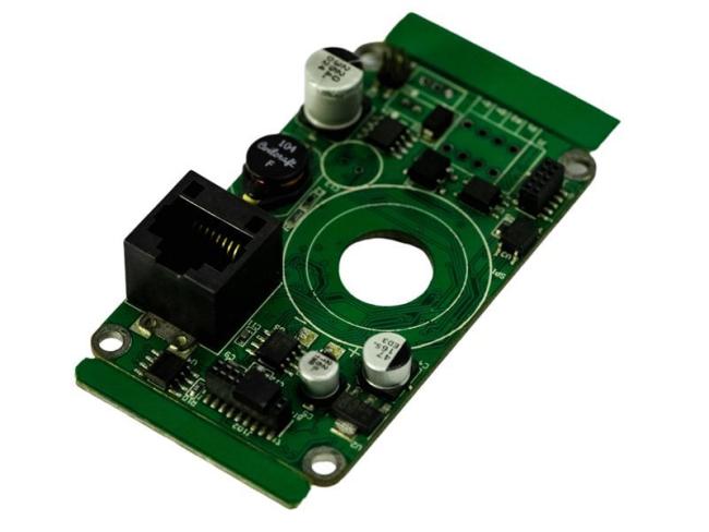
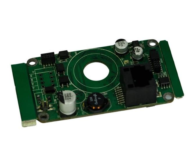
6-16 layer high-frequency PCB assembly designed for IoT applications and hotel communication systems, supporting full turnkey service from design to production.
- 6-16 layer FR-4 construction with 0.2mm minimum hole size
- 4-6mil trace width/spacing for optimal signal integrity
- ENIG/immersion silver finishes for superior corrosion resistance
- Advanced materials including Rogers and high-Tg FR4 (≥170°C)
- Supports RS485, Ethernet, Zigbee, and Modbus protocols
- RS485 differential signaling ensures stable communication up to 1200 meters
- Seamless integration with hotel PBX systems, IP TVs, and smart controls
| Parameter | Specification |
|---|---|
| Board Thickness | 0.8 - 2.4mm |
| Line Width/Spacing | 0.1 - 0.3mm / 0.1 - 0.3mm |
| Operating Temperature | -40°C to 85°C |
| Signal Frequency | kHz to GHz range depending on application |
| Insulation Resistance | ≥1000MΩ |
100% Electronic Testing: Rigorous ICT, FCT, and thermal shock testing (288°C for 10 seconds) ensures compliance with IPC-A-610 standards.
Global Compliance: FCC SDoC/FCC ID, CE, ISO 9001, IATF 16949, and RoHS certifications.
2-48 layer boards with blind/buried vias, 3/3mil trace/spacing, ±7% impedance control for 5G, industrial control, medical, and automotive applications.
Full turnkey solutions including PCB fabrication, component sourcing, SMT assembly, and functional testing.
X-ray inspection, AOI testing, impedance testing, and thermal cycling with defect rate <0.2%.


Full lifecycle support from schematic design to mass production with rapid prototyping (24-hour turnaround for small batches) and scalable production for bulk orders.
Note: All products are custom services. Please contact our customer service before ordering to confirm product details.

Get in Touch
Have questions about our products or want to discuss a custom order? Our team is ready to help you.