Custom Communication PCB Assembly for 5G Systems - 6-16 Layer FR-4 with 0.2mm Hole Size
Price:
negotiable
MOQ:
1unit
Delivery Time:
10-15 working days
Brand:
Ring PCBA ,support OEM
Product Description
High-Performance Communication Equipment PCB Assembly
Custom PCBA solutions engineered for 5G infrastructure, telecom systems, and data network devices with superior signal integrity and thermal management.
Key Features & Technical Advantages
High-Frequency Performance
Optimized for 4G/5G and Wi-Fi applications with minimal signal loss using Rogers and high-Tg FR4 materials (≥170°C).
- 6-16 layer FR-4 construction
- 0.2mm minimum hole size
- 4-6mil trace width/spacing
- ENIG/immersion silver finishes
- 100% electronic testing (ICT, FCT, thermal shock)
Robust Thermal Management
Engineered for prolonged operation with optimized thermal dissipation using high-Tg materials and multi-layered designs.
Multi-Protocol Compatibility
Supports RS485, Ethernet, Zigbee, and Modbus protocols for seamless integration with hotel PBX systems and smart controls.
RS485 differential signaling ensures stable communication up to 1200 meters.
Customization Excellence
- Full lifecycle support from schematic to mass production
- Material options: FR-4, Rogers, Teflon
- Surface finishes: HASL (lead-free), OSP, immersion silver
- 24-hour rapid prototyping for small batches
Technical Specifications
| Parameter | Specification |
|---|---|
| Board Thickness | 0.8 - 2.4mm |
| Line Width/Spacing | 0.1 - 0.3mm / 0.1 - 0.3mm |
| Surface Finish | ENIG, HASL, immersion silver |
| Operating Temperature | -40°C - 85°C |
| Signal Frequency | kHz to GHz range |
| Component Density | High density with dozens to hundreds per square inch |
| Assembly Accuracy | ±0.05 - 0.1mm tolerance |
Manufacturing Capabilities
17 years of experience serving 20,000+ customers worldwide with comprehensive PCB and PCBA services.
Advanced Engineering Solutions
- 2-48 layer boards with blind/buried vias
- 3/3mil trace/spacing with ±7% impedance control
- HDI PCB manufacturing with microvias and fine-pitch technology
- 8-stage lead-free reflow soldering and wave soldering
Quality Assurance & Certifications
- ISO9001, IATF16949, RoHS compliance
- FCC SDoC/FCC ID and CE certification
- IPC-A-610 Class 2/3 standards
- Defect rate
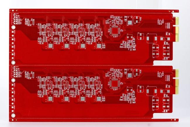
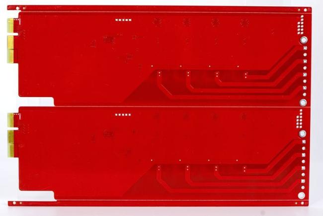
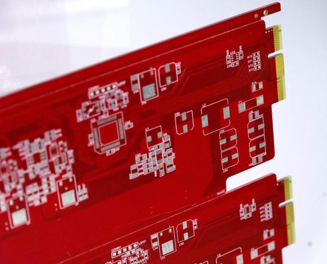
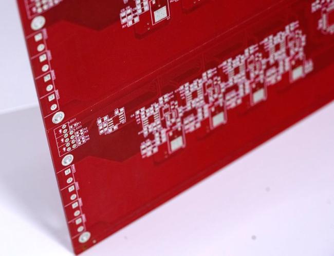
Product Images
For custom communication equipment PCBA requirements, please provide your technical specifications or drawings for professional consultation.
Similar Products

Get in Touch
Have questions about our products or want to discuss a custom order? Our team is ready to help you.
Company
Ring PCB Technology Co.,Limited
Location
Building 36A,Longwangmiao Industrial park, Baishixia Community, Fuyong Street, Bao'an District, Shenzhen,China
Contact Person
Michelle Law