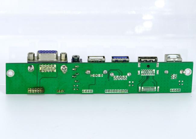
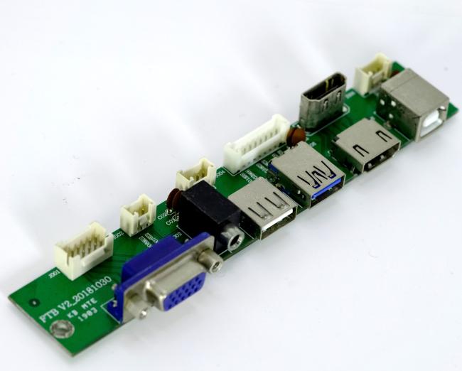
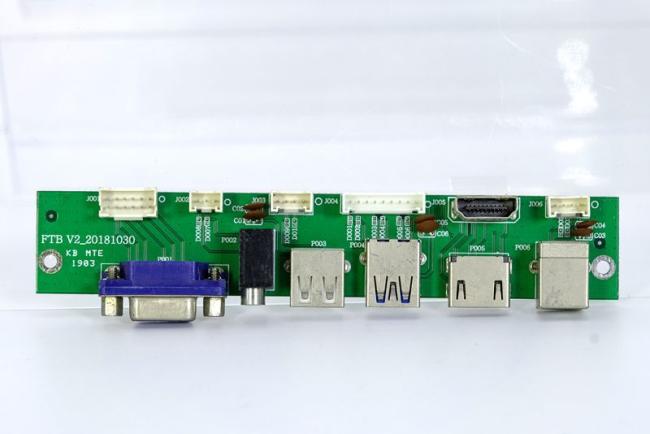
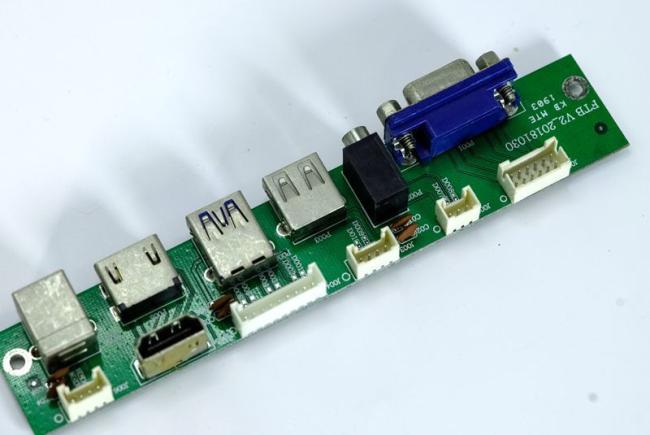
Custom Communication Device PCB Assembly - 2-20+ Layer Telecom PCBA with 3-Day Prototype & 7-Day Production
Ring PCB specializes in telecom and network PCB assembly, delivering customized PCBA solutions based on client specifications. Our expertise ensures stable signal transmission, enhanced durability, and cost-effective production for 5G, IoT, and smart communication devices.
- Custom manufacturing based on client drawings and requirements
- High signal integrity with minimized interference
- Durable materials with controlled impedance capabilities
- Efficient heat dissipation for high-frequency devices
- Full-turnkey services from design to mass production
- Certified quality with ISO9001, ISO14001, ISO13485, IATF16949 compliance
| Parameter | Specification Range | Notes |
|---|---|---|
| PCB Layers | 2 - 20+ layers | Supports complex multi-layer designs |
| Board Thickness | 0.4 - 3.2 mm | Customized per device requirements |
| Copper Thickness | 1 - 6 oz | High-current carrying capability |
| Surface Finish | HASL, ENIG, OSP, Immersion Silver, Hard Gold | Ensures durability and solderability |
| Impedance Control | ±5% | Essential for high-frequency signals |
| Component Mounting | SMT, Through-Hole, Mixed Assembly | Full flexibility for various devices |
| Testing | ICT, Flying Probe, Functional Test | Ensures 100% product reliability |
| Production Lead Time | Prototype in 3 days, Mass production in 7 days | Fast delivery to meet market demand |
- 5G base stations and network equipment
- IoT devices and smart meters
- Wireless routers, modems and gateways
- Telecommunication infrastructure systems
- Satellite and radio communication devices
- 17 years of industry experience in PCB assembly
- Customized production based on client drawings
- 500+ skilled employees ensuring high-quality output
- Two modern factories in Shenzhen and Zhuhai covering 5000+㎡
- Fast turnaround with 3-day prototyping and 7-day mass production
- Global service with products exported to over 50 countries
- Full customization from PCB manufacturing to complete PCBA assembly
It is the process of producing PCBs for telecom, IoT, and networking devices. High-quality PCB assembly ensures signal stability, impedance control, and long-term reliability.
Yes, we specialize in custom communication device PCB assembly according to client drawings and requirements, supporting high-frequency and multi-layer PCBA designs.
We provide ISO9001, ISO14001, ISO13485, and IATF16949 certified production with 100% testing, including ICT, flying probe, and functional testing.
We offer rapid prototyping in 3 days and batch production in 7 days, meeting urgent communication device PCBA needs worldwide.
At Ring PCB, we deliver customized communication device PCB assembly solutions tailored to your drawings and requirements. With certified quality, fast turnaround, and global service, we are your reliable partner in telecom and network PCBA manufacturing.
Contact us at info@ringpcb.com or visit www.turnkeypcb-assembly.com to start your communication device PCB assembly project with Ring PCB!

Get in Touch
Have questions about our products or want to discuss a custom order? Our team is ready to help you.