Turnkey Communication Device PCB Assembly With Fast Prototyping ISO Certified PCBA Factory
Reliable Telecom PCB Assembly Services | ISO Certified Factory
Introduction
At Ring PCB, we specialize in communication device PCB assembly (also known as telecom PCB assembly or network PCB assembly), delivering customized PCBA solutions based on client drawings and requirements. With the rapid development of 5G, IoT, and smart devices, communication equipment requires precise, durable, and high-performance PCB assemblies. Our expertise ensures stable signal transmission, enhanced durability, and cost-effective production.
Key Features & Advantages
-
Custom Manufacturing Based on Drawings – Tailored PCB assembly solutions for all communication devices.
-
High Signal Integrity – Minimized interference for stable performance.
-
Durable & Reliable Materials – Advanced laminates with controlled impedance.
-
Efficient Heat Dissipation – Optimized thermal design for high-frequency devices.
-
Full-Turnkey Services – From design, prototyping to mass production.
-
Certified Quality – ISO9001, ISO14001, ISO13485, IATF16949 compliance.
Technical Challenges in Communication Device PCB Assembly
-
High-frequency signal transmission requires strict impedance control.
-
Multi-layer miniaturized design for compact communication devices.
-
Advanced thermal management for high-power equipment.
-
Rigorous testing to guarantee stable performance across environments.
Common Technical Parameters
| Parameter | Specification Range | Notes |
|---|---|---|
| PCB Layers | 2 – 20+layers | Supports complex multi-layer designs |
| Board Thickness | 0.4 – 3.2 mm | Customized per device requirements |
| Copper Thickness | 1 – 6 oz | High-current carrying capability |
| Surface Finish | HASL, ENIG, OSP, Immersion Silver, Hard Gold | Ensures durability & solderability |
| Impedance Control | ±5% | Essential for high-frequency signals |
| Component Mounting | SMT, Through-Hole, Mixed Assembly | Full flexibility for various devices |
| Testing | ICT, Flying Probe, Functional Test | Ensures 100% product reliability |
| Production Lead Time | Prototype in 3 days, Mass production in 7 days | Fast delivery to meet market demand |
The above common technical parameters are for reference only. If you need to customize other communication equipment PCBA, please contact our professional customer service in time for consultation.
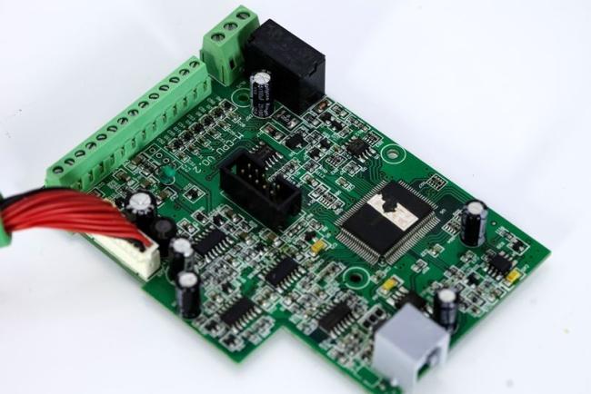
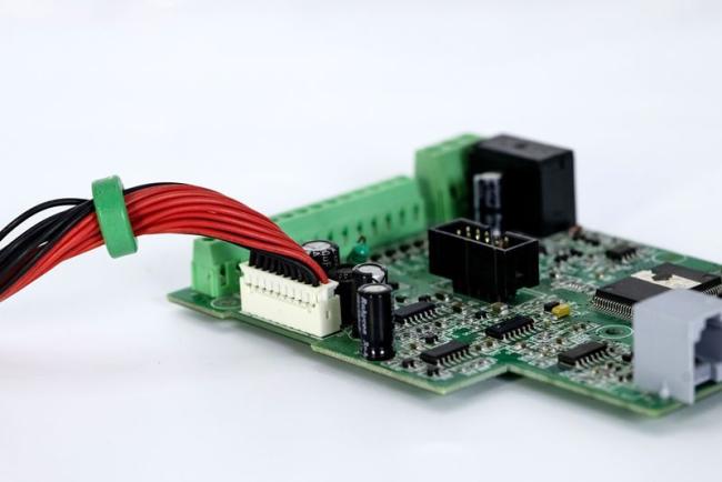
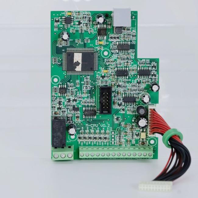
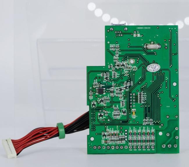
This is the PCB assembly of the customized power relay station monitoring board for your reference.
Application Fields
Our communication device PCB assemblies are widely applied in:
-
5G base stations & network equipment
-
IoT devices & smart meters
-
Wireless routers, modems & gateways
-
Telecommunication infrastructure systems
-
Satellite and radio communication devices
Why Choose Ring PCB?
With 17 years of industry experience, Ring PCB is your trusted partner for communication device PCB assembly and turnkey PCBA services.
-
Customized production based on client drawings.
-
500+ skilled employees ensuring high-quality output.
-
Two modern factories in Shenzhen and Zhuhai, covering 5000+㎡.
-
Fast turnaround – 3 days for prototyping, 7 days for mass production.
-
Global service – Products exported to over 50 countries.
-
Full customization – From PCB manufacturing to complete PCBA assembly.
FAQ from Ring PCB
Q1: What is Communication Device PCB Assembly and why is it important?
A1: It is the process of producing PCBs for telecom, IoT, and networking devices. High-quality PCB assembly ensures signal stability, impedance control, and long-term reliability.
Q2: Can Ring PCB provide custom PCB assembly based on my drawings?
A2: Yes, we specialize in custom communication device PCB assembly according to client drawings and requirements, supporting high-frequency and multi-layer PCBA designs.
Q3: What certifications and testing are available?
A3: We provide ISO9001, ISO14001, ISO13485, and IATF16949 certified production with 100% testing, including ICT, flying probe, and functional testing.
Q4: How fast can you deliver?
A4: We offer rapid prototyping in 3 days and batch production in 7 days, meeting urgent communication device PCBA needs worldwide.
Ready to Start Your Communication Device PCB Assembly Project?
At Ring PCB, we deliver customized communication device PCB assembly solutions tailored to your drawings and requirements. With certified quality, fast turnaround, and global service, we are your reliable partner in telecom and network PCBA manufacturing.
Contact us at info@ringpcb.com or visit www.turnkeypcb-assembly.com to start your communication device PCB assembly project with Ring PCB!

Get in Touch
Have questions about our products or want to discuss a custom order? Our team is ready to help you.