
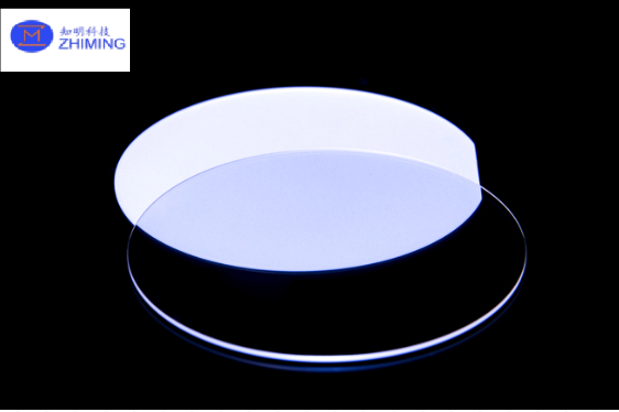
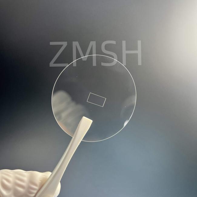
Sapphire Wafer Monocrystal Al2O3 DSP SSP 2inch 4inch 6inch 8inch 12inch A plane C plane
Sapphire Wafer Monocrystal Al2O3 DSP SSP 2inch 4inch 6inch 8inch 12inch A plane C plane
Description:
Sapphire substrates are widely used in the production of III-V nitrides, superconductors, and magnetic epitaxial films due to their low lattice mismatch and excellent physical and chemical stability. They are extensively employed in non-polar and semi-polar epitaxial growth of materials such as GaN, ZnO, AlN, various semiconductor thin film epitaxial growth processes, Silicon On Sapphire technology, optical windows, and more.
We use only optical-grade single crystal materials, and all raw materials are sourced from 99.999% high-purity single crystal Al2O3. Our sapphire substrates have superior surface roughness, flatness, and cleanliness, making them suitable for semiconductor thin film epitaxial growth, optical windows, and other high-tech applications.

Character
1. High optical transparency
Sapphire wafer with its high optical transparency, finds widespread applications as a dielectric material in microelectronic tubes, ultrasonic transducers, waveguide laser cavities, and other optical components. It serves as a window material for infrared military devices,spacecraft, high-power lasers, and optical communication systems.
2. High hardness, strength, high operating temperature, wear resistance, and corrosion resistance
Sapphire wafer is valued for its high hardness, strength, high operating temperature, wear resistance, and corrosion resistance, making it suitable for harsh environments. It is commonly used in applications such as boiler water gauges (high-temperature resistance), barcode scanners, precision bearings (wear resistance), coal and natural gas industries, oil well sensing sensors, and detector windows (corrosion resistance).
3. Electrical insulation, transparency, good thermal conductivity
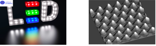
Sapphire wafer, known for its electrical insulation, transparency, good thermal conductivity, and high hardness, can serve as a substrate material for LEDs, microelectronic circuits, ultra-high-speed integrated circuits, and other integrated circuits.
| Hardness | Knoop: 1500 |
| Mohs: 9 | |
| Tensile Strength | 275 - 400 MPa |
| 40,000 - 58,000 psi | |
| Flexural Strength | 480 - 895 MPa |
| 70,000 - 130,000 psi | |
| Compression Strength (ultimate) | 2.0 GPa / 300,000 psi |
| Young's Modulus (elasticity) | 345 GPa / 50 x 106 psi |
| Bulk Modulus (compression) | 250 GPa / 36 x 106 psi |
| Shear Modulus (rigidity) | 145 GPa / 21 x 106 psi |
| Modulus of Rupture | 350 - 690 MPa / 50,000 - 100,000 psi |
| Melting Point | 2040°C / 3700°F / 2310 K |
Applications:
1. Microelectronic IC applications, especially ultra-high-speed integrated circuits (SOS), typically involve heteroepitaxial silicon grown on R-plane (1-102) sapphire wafers.
2. Hybrid microelectronics: Hybrid microelectronic products mainly include HIC and MCM, which have high wafer requirements.
3. Sapphire wafers, known for stable dielectric constants and low dielectric losses, are the most commonly used substrates for HIC and the primary substrates for MCM. Usually, the A-plane (11-20) sapphire substrates are employed.
FAQ:
Q: What is the size of the Sapphire substrate?
A: The size of the Sapphire substrate can be customized based on your needs.
Q: What are the applications of the Sapphire substrate?
A: The Sapphire substrate has a wide range of applications, such as in LED, semiconductor, optical, and electronic industries.
Product recommend
1. 2 Inch Monocrystalline Sapphire Wafer Double Sides Polished Al2O3 99.999% Single Crystal Substrate
2.6inch 8inch 12inch Sapphire Wafer With Excellent Chemical Stability DSP Surface
Customization:
We can provide high-quality surface states of any crystal orientation (C, A, R, M, etc.). In addition to round sapphire wafers, square and rectangular wafers are also available. We offer sapphire wafers in various sizes, such as 5mm x 5mm, 10mm x 10mm, 10mm x 15mm, 15mm x 20mm, etc.
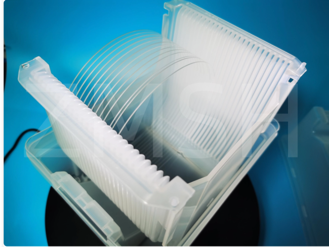
Packing: 25 piece/box or single piece box packaging maximizes customer research flexibility.
Get in Touch
Have questions about our products or want to discuss a custom order? Our team is ready to help you.