
N-GaAs Substrate 6inch 350um Thickness For VCSEL Use OptiWave VCSEL EpiWafer
N-GaAs substrate 6inch 350um thickness for VCSEL use OptiWave VCSEL epiWafer
VCSEL epiWafer N-GaAs substrate' s abstract
The VCSEL epiWafer on N-GaAs substrate is designed for high-performance optical applications, particularly for Gigabit Ethernet and digital data link communication. Built on a 6-inch wafer, it features a high uniformity laser array and supports center optical wavelengths of 850 nm and 940 nm. The structure is available in either oxide-confined or proton implant VCSEL configurations, ensuring flexibility in design and performance. The wafer is optimized for applications requiring low dependence on electrical and optical characteristics over temperature, making it ideal for use in laser mice, optical communication, and other temperature-sensitive environments.
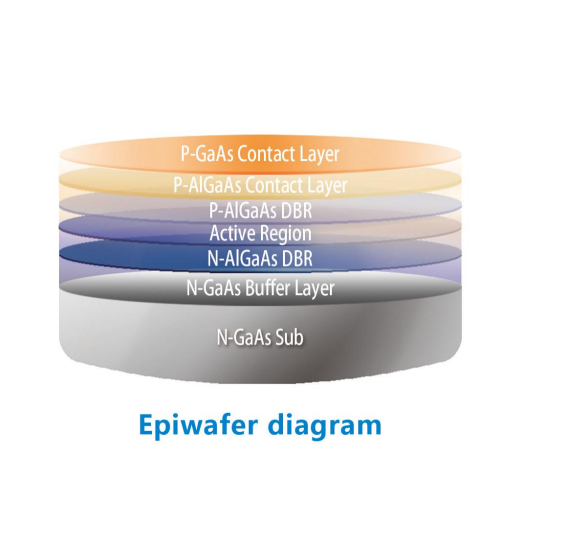
VCSEL epiWafer N-GaAs substrate's structure
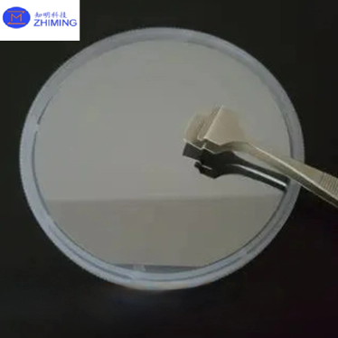
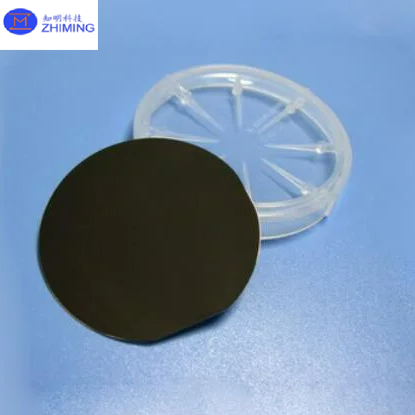
VCSEL epiWafer N-GaAs substrate' s photo
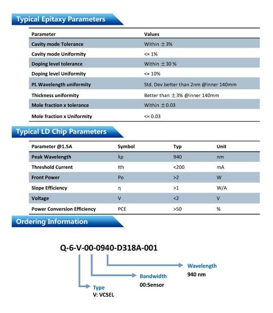
VCSEL epiWafer N-GaAs substrate' s datasheet
VCSEL epiWafer N-GaAs substrate' s properties
The VCSEL epiWafer on N-GaAs substrate has several key properties that make it suitable for high-performance optical applications:
N-GaAs Substrate:
- Provides excellent electrical conductivity and serves as a stable base for the epitaxial growth of VCSEL structures.
- Offers low defect density, which is crucial for high-performance and reliable device operation.
Wavelength Tunability:
- Supports 850 nm and 940 nm center optical wavelengths, making it ideal for applications in optical communication and 3D sensing.
High Uniformity Laser Array:
- Ensures consistent performance across the wafer, crucial for array-based devices in data centers and fiber optic networks.
Oxide-Confined or Proton Implant:
- Available in oxide-confined or proton implant VCSEL structures, offering flexibility in design to optimize performance for specific applications.
Thermal Stability:
- Designed to exhibit low dependence on electrical and optical characteristics over a wide temperature range, ensuring stable operation in temperature-sensitive environments.
High Power and Speed:
- The wafer's structure supports high-speed data transmission and high-power operation, making it suitable for Gigabit Ethernet, data communication, and LIDAR systems.
Scalability:
- The 6-inch wafer format allows for cost-effective production, supporting large-scale manufacturing and integration into various optical systems.
These properties make the VCSEL epiWafer on N-GaAs substrate ideal for applications requiring high efficiency, temperature stability, and reliable performance.
Get in Touch
Have questions about our products or want to discuss a custom order? Our team is ready to help you.