
Si Wafer 8inch Tickness 675 Μm To 775 ΜmP Type N Type 111 Double Side Polished / Single Side Polished
8inch Si Wafer Si Substrate 111 P Type N Type for Micro-electromechanical systems (MEMS) Or Power semiconductor devices Or Optical components and sensors
Product Description: The 8-inch silicon wafer with (111) crystal orientation is a high-quality, single-crystal material widely used in semiconductor manufacturing. The (111) crystal orientation provides specific electrical and mechanical properties that are beneficial for various high-performance applications.
Key Features:
- Diameter: 8 inches (200 mm).
- Crystal Orientation: (111), offering unique surface properties, ideal for certain semiconductor processes and device characteristics.
- High Purity: Manufactured with a high level of purity to ensure uniformity and low defect rates, critical for semiconductor and microelectronics applications.
- Surface Quality: Typically polished or cleaned to meet stringent surface requirements for device manufacturing.
Applications:
- Power Semiconductor Devices: The (111) orientation is preferred in certain power devices due to its high breakdown voltage and favorable thermal properties.
- MEMS (Microelectromechanical Systems): Often used for sensors, actuators, and other micro-scale devices, thanks to its well-defined crystal structure.
- Optoelectronic Devices: Suitable for applications in light-emitting devices and photodetectors, where high crystal quality is important.
- Solar Cells: (111)-oriented silicon is also used in high-efficiency photovoltaic cells, benefiting from enhanced light absorption and carrier mobility.
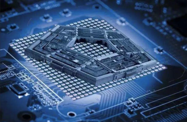
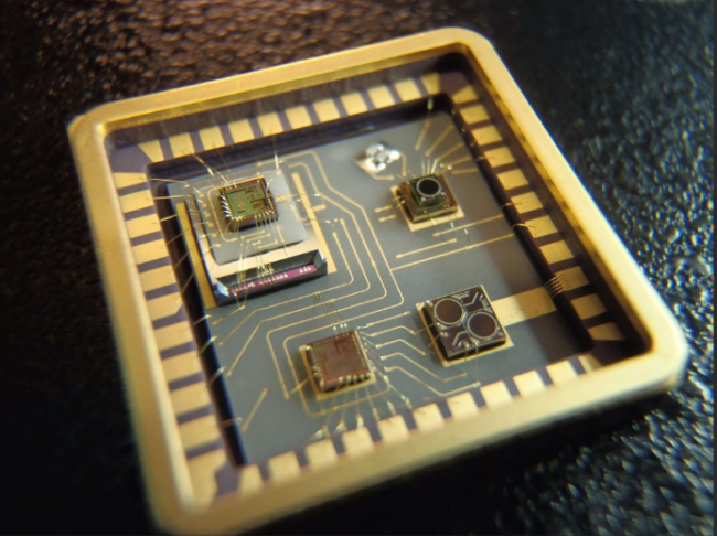
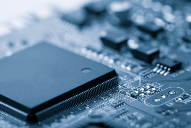
Application picture of Si Wafer:

Customizations:
- Thickness and Resistivity: These can be tailored according to customer specifications to meet specific application requirements.
- Doping Type: P-type or N-type doping is available to adjust the wafer’s electrical characteristics.
This silicon wafer type is crucial for a wide range of semiconductor applications, providing a balance of mechanical strength, electrical performance, and ease of processing.
Get in Touch
Have questions about our products or want to discuss a custom order? Our team is ready to help you.