
12inch SiC Wafer Silicon Carbide Wafer 300mm Substrate 750±25um 4H-N Type Orientation 100 Production Research Grade
12inch SiC wafer Silicon Carbide wafer 300mm 750±25um 4H-N type orientation 100 Production Research grade
12inch SiC wafer's abstract
This 12-inch Silicon Carbide (SiC) wafer is designed for advanced semiconductor applications, featuring a 300mm diameter, 750±25µm thickness, and a 4H-N type crystal orientation with a polytype of 4H-SiC. The wafer is produced using high-quality manufacturing techniques to meet the standards of research-grade and production environments. Its robust properties make it well-suited for high-power, high-temperature, and high-frequency devices, often used in applications such as electric vehicles (EVs), power electronics, and RF technology. The wafer’s superior structural integrity and precise specifications ensure high yields in device fabrication, offering optimal performance in cutting-edge research and industrial applications.
12inch SiC wafer's data chart
| 1 2 inch Silicon Carbide (SiC) Substrate Specification | |||||
| Grade | ZeroMPD Production Grade(Z Grade) |
Standard Production Grade(P Grade) |
Dummy Grade (D Grade) |
||
| Diameter | 3 0 0 mm | ||||
| Thickness | 4H-N | 750μm±15 μm | 750μm±25 μm | ||
| 4H-SI | 750μm±15 μm | 750μm±25 μm | |||
| Wafer Orientation | Off axis : 4.0° toward <1120 >±0.5° for 4H-N, On axis : <0001>±0.5° for 4H-SI | ||||
| Micropipe Density | 4H-N | ≤0.4cm-2 | ≤4cm-2 | ≤25cm-2 | |
| 4H-SI | ≤5cm-2 | ≤10cm-2 | ≤25cm-2 | ||
| Resistivity | 4H-N | 0.015~0.024 Ω·cm | 0.015~0.028 Ω·cm | ||
| 4H-SI | ≥1E10 Ω·cm | ≥1E5 Ω·cm | |||
| Primary Flat Orientation | {10-10} ±5.0° | ||||
| Primary Flat Length | 4H-N | N/A | |||
| 4H-SI | Notch | ||||
| Edge Exclusion | 3 mm | ||||
| LTV/TTV/Bow /Warp | ≤5μm/≤15μm/≤35 μm/≤55 μm | ≤5μm/≤15μm/≤35 □ μm/≤55 □ μm | |||
| Roughness | Polish Ra≤1 nm | ||||
| CMP Ra≤0.2 nm | Ra≤0.5 nm | ||||
| Edge Cracks By High Intensity Light Hex Plates By High Intensity Light Polytype Areas By High Intensity Light Visual Carbon Inclusions Silicon Surface Scratches By High Intensity Light |
None Cumulative area ≤0.05% None Cumulative area ≤0.05% None |
Cumulative length ≤ 20 mm, single length≤2 mm Cumulative area ≤0.1% Cumulative area≤3% Cumulative area ≤3% Cumulative length≤1×wafer diameter |
|||
| Edge Chips By High Intensity Light | None permitted ≥0.2mm width and depth | 7 allowed, ≤1 mm each | |||
| (TSD) Threading screw dislocation | ≤500 cm-2 | N/A | |||
| (BPD) Base plane dislocation | ≤1000 cm-2 | N/A | |||
| Silicon Surface Contamination By High Intensity Light | None | ||||
| Packaging | Multi-wafer Cassette Or Single Wafer Container | ||||
| Notes: | |||||
| 1 Defects limits apply to entire wafer surface except for the edge exclusion area. 2The scratches should be checked on Si face only. 3 The dislocation data is only from KOH etched wafers. |
|||||
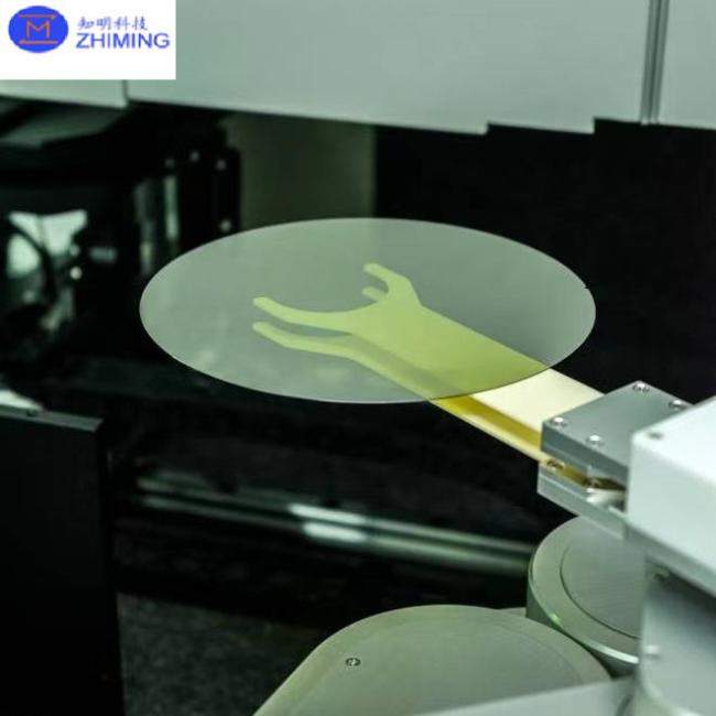
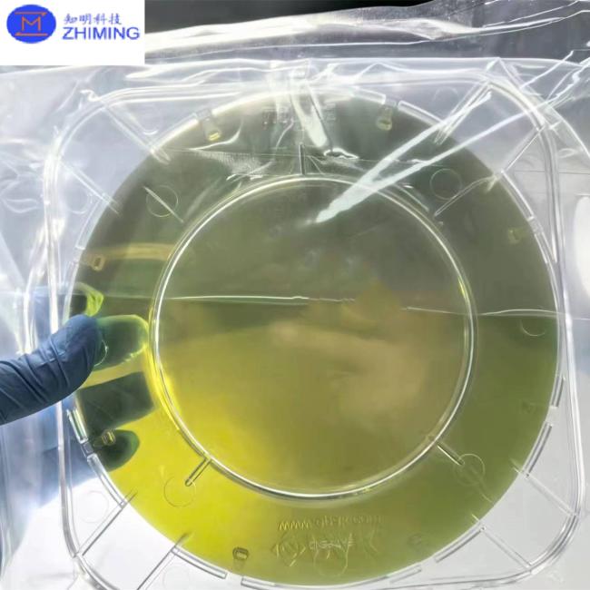
12inch SiC wafer's photo
12inch SiC wafer's properties
1. Material Properties of SiC:
- Wide Bandgap: SiC has a wide bandgap (~3.26 eV), allowing it to operate at higher voltages, temperatures, and frequencies compared to traditional silicon (Si).
- High Thermal Conductivity: SiC's thermal conductivity is much higher than silicon (about 3.7 W/cm·K), making it well-suited for high-power applications where heat dissipation is critical.
- High Breakdown Voltage: SiC can handle much higher voltages (up to 10 times higher than silicon), making it ideal for power electronics, such as power transistors and diodes.
- High Electron Mobility: The electron mobility in SiC is higher than in traditional silicon, contributing to faster switching times in electronic devices.
2. Mechanical Properties:
- High Hardness: SiC is very hard (Mohs hardness of 9), which contributes to its wear resistance but also makes it difficult to process and machine.
- Stiffness: It has a high Young's modulus, meaning it is stiffer and more durable compared to silicon, which enhances its robustness in devices.
- Brittleness: SiC is more brittle than silicon, which is important to consider during wafer processing and device manufacturing.
12inch SiC wafer's applications
12-inch SiC wafers are primarily used in high-performance power electronics, including power MOSFETs, diodes, and IGBTs, enabling efficient energy conversion in industries such as electric vehicles, renewable energy, and industrial power systems. SiC’s high thermal conductivity, wide bandgap, and ability to withstand high temperatures make it ideal for applications in automotive electronics, power inverters, and high-power energy systems. Its use in high-frequency RF devices and microwave communication systems also makes it critical for telecommunications, aerospace, and military radar systems.
Additionally, SiC wafers are used in LED and optoelectronics, serving as substrates for blue and UV LEDs, which are crucial for lighting, displays, and sterilization. The material's resilience in harsh environments enables its use in high-temperature sensors, medical devices, and satellite power systems. With its growing role in smart grids, energy storage, and power distribution, SiC is helping to improve efficiency, reliability, and performance across a wide range of applications.
12inch SiC wafer's Q&A
1. What is a 12-inch SiC wafer?
Answer: A 12-inch SiC wafer is a silicon carbide (SiC) substrate with a diameter of 12 inches, primarily used in the semiconductor industry, especially for high-power, high-temperature, and high-frequency applications. SiC materials are widely used in power electronics, automotive electronics, and energy conversion devices due to their excellent electrical, thermal, and mechanical properties.
2. What are the advantages of a 12-inch SiC wafer?
Answer: The advantages of a 12-inch SiC wafer include:
- High Temperature Stability: SiC can operate at temperatures up to 600°C or higher, offering better high-temperature performance than traditional silicon materials.
- High Power Handling: SiC can withstand high voltage and current, making it suitable for high-power applications such as electric vehicle battery management and industrial power supplies.
- High Thermal Conductivity: SiC has a significantly higher thermal conductivity compared to silicon, which helps in better heat dissipation, improving device reliability and efficiency.
Get in Touch
Have questions about our products or want to discuss a custom order? Our team is ready to help you.