
Precision Ultra Thin Diamond Wire For Semiconductor PV Silicon Wafer Slicing
Precision Ultra-Thin Diamond Wire For Semiconductor & PV Silicon Wafer Slicing
Description For Precision Ultra-Thin Diamond Wire For Semiconductor & PV Silicon Wafer Slicing:
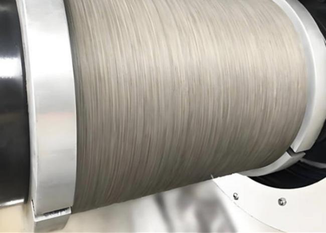
Precision ultra-thin diamond wire is a cutting-edge cutting tool used in the semiconductor and photovoltaic (PV) industries for slicing silicon wafers with exceptional accuracy and minimal material loss. It consists of a high-tensile core wire (typically steel or tungsten) electroplated with diamond abrasive particles, enabling ultra-thin, high-efficiency slicing of monocrystalline and polycrystalline silicon ingots.
Features For Precision Ultra-Thin Diamond Wire For Semiconductor & PV Silicon Wafer Slicing:
1. Ultra-Thin Diameter: Ranges from 30–100 μm, enabling minimal kerf loss and higher wafer yield.
2. High Precision Cutting: Ensures uniform wafer thickness (as low as 100–200 μm) with superior surface quality.
3. Diamond Abrasives: Synthetic diamond particles (5–30 μm) provide exceptional hardness and wear resistance.
4. High Tensile Core: Steel or tungsten wire ensures durability and breakage resistance during high-speed cutting.
5. Low Wire Vibration: Enhances cutting stability, reducing wafer surface defects like micro-cracks.
Applications For Precision Ultra-Thin Diamond Wire For Semiconductor & PV Silicon Wafer Slicing:
1. Semiconductor Industry: Slicing silicon ingots into ultra-thin wafers for ICs, MEMS, and power devices. Enables thinner wafers for advanced packaging (e.g., 3D ICs).
2. Photovoltaic (PV) Solar Cells:Cutting monocrystalline and polycrystalline silicon ingots into wafers for high-efficiency solar panels. Reduces silicon waste, lowering production costs.
3. Advanced Materials Processing: Used for slicing brittle materials like sapphire, SiC, and glass.
Advantages For Precision Ultra-Thin Diamond Wire For Semiconductor & PV Silicon Wafer Slicing:
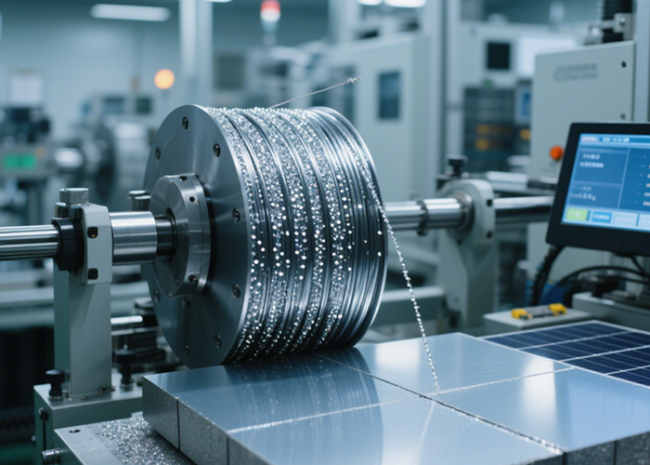
1. Higher Efficiency: Faster cutting speeds (up to 1.5–2.5 m/s) compared to slurry-based multi-wire sawing.
2. Lower Material Waste: Kerf loss reduced to ~100 μm (vs. 150–200 μm with slurry saws).
3. Eco-Friendly: Eliminates slurry waste, reducing environmental impact.
Cost-Effective: Longer wire lifespan and higher productivity lower overall manufacturing costs.
Get in Touch
Have questions about our products or want to discuss a custom order? Our team is ready to help you.