
2 Sided Aluminum PCB Assembly Service Through Hole Component Assembly
2 Sided PCB Assembly Advanced Circuits Assembly Aluminum PCB Assembly
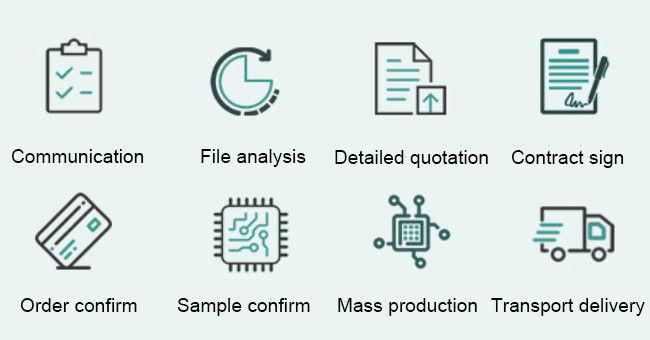
YDY could provide one-stop pcb assembly service, including:
- Engineering Services
- PCB Design & Assembly
- Component Procurement & Material Management
- Fast Track Prototyping
- Cable and Wire Assemblies
- Plastics and Molds
PCB Assembly(SMT) Product Capacity
| Turnkey PCBA | PCB+components sourcing+assembly+package |
| Assembly details | SMT and Thru-hole, ISO SMT and DIP lines |
| Lead Time | Prototype: 15 work days. Mass order: 20~25 work days |
| Testing on products | Flying Probe Test, X-ray Inspection, AOI Test, Functional test |
| Quantity | Min quantity: 1pcs. Prototype, small order, mass order, all OK |
| Files needed | PCB: Gerber files(CAM, PCB, PCBDOC) |
| Components: Bill of Materials(BOM list) | |
| Assembly: Pick-N-Place file | |
| PCB Panel Size | Min size: 0.25*0.25 inches(6*6mm) |
| Max size: 20*20 inches(500*500mm) | |
| PCB Solder Type | Water Soluble Solder Paste, RoHS lead free |
| Components details | Passive Down to 0201 size |
| BGA and VFBGA | |
| Leadless Chip Carriers/CSP | |
| Double-sided SMT Assembly | |
| Fine Pitch to 0.8mils | |
| BGA Repair and Reball | |
| Part Removal and Replacement | |
| Component package | Cut Tape,Tube,Reels,Loose Parts |
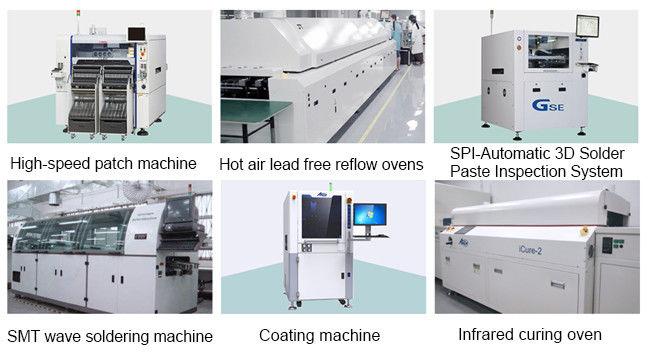
| PCB assembly process |
Drilling-----Exposure-----Plating-----Etaching & Stripping-----Punching-----Electrical Testing-----SMT-----Wave Soldering-----Assembling-----ICT-----Function Testing-----Temperature & Humidity Testing |
PCB Manufacturing Process
1.1 Step 1 – The Design
1.2 Step 2 – Printing the Design
1.3 Step 3 – Creating the Substrate
1.4 Step 4 – Printing the Inner Layers
1.5 Step 5 – Ultraviolet Light
1.6 Step 6 – Removing Unwanted Copper
1.7 Step 7 – Inspection
1.8 Step 8 – Laminating the Layers
1.9 Step 9 – Pressing the Layers
1.10 Step 10 – Drilling
1.11 Step 11 – Plating
1.12 Step 12 – Outer Layer Imaging
1.13 Step 13 – Plating
1.14 Step 14 – Etching
1.15 Step 15 – Solder Mask Application
1.16 Step 16 – Silkscreening
1.17 Step 17 – Surface Finish
1.18 Step 18 – Testing
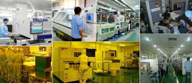
With our many years of experience,we have built an excellent core team from PCB processing,compent procurement,SMT assembly and finished product testing.We try our best to serve every company.We will always
uphold our service philosophy.win-win,efficient and convenience.
Shenzhen Yideyi Technology Co., Ltd. completes factory production system and strict quality requirements have helped hundreds of customers finished successful projects.
YDY has a dedicated team of professionals to guide you at every step - from sourcing to overcoming any potential challenges along the way.
The most important is the reliable material procurement channel would help you to minimize BOM costs.
Get in Touch
Have questions about our products or want to discuss a custom order? Our team is ready to help you.