
Ems Contract PCB Assembly Service China Through Hole Pad Pcb
Contract Manufacturing Pcb Assembly Custom Pcb Assembly Service
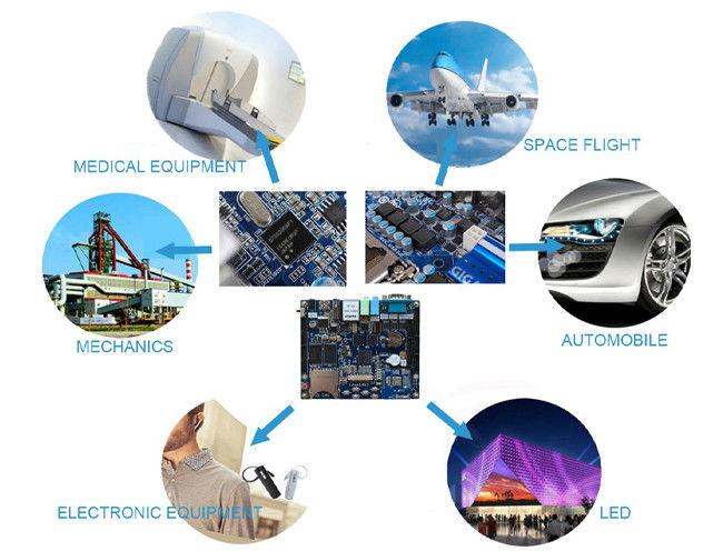
Shenzhen Yideyi Technology Co., Ltd. strives to be your one stop solution partner in EMS supply chain, including PCB design , PCB fabrication and PCB assembly (PCBA).
We provide some of the most advanced PCB technology, including HDI PCBs,multilayer PCBs, Rigid-Flexible PCBs.
We can support from quick turn prototype to medium & mass Production.
In general, our global customers are very impressed with our services: rapid response, competitive price and quality commitment.Providing more valuable technical service and overall solution is the way YDY forward.
Looking to the future, YDY will concentrate on the innovation and development of electronics manufacturing technology as always, and make persistent efforts on PCB & PCBA one-stop service to provide first-class services and create more value for our customers
YDY could provide one-stop pcb assembly service, including:
- Engineering Services
- PCB Design & Assembly
- Component Procurement & Material Management
- Fast Track Prototyping
- Cable and Wire Assemblies
- Plastics and Molds

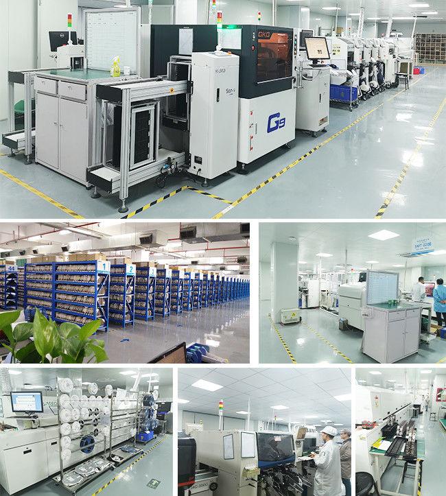
PCB Assembly(SMT) Product Capacity:
| Turnkey PCBA | PCB+components sourcing+assembly+package |
| Assembly details | SMT and Thru-hole, ISO SMT and DIP lines |
| Testing on products | Flying Probe Test, X-ray Inspection, AOI Test, Functional test |
| Quantity | Min quantity: 1pcs. Prototype, small order, mass order, all OK |
| Files needed | PCB: Gerber files(CAM, PCB, PCBDOC) |
| Components: Bill of Materials(BOM list) | |
| Assembly: Pick-N-Place file | |
| PCB Panel Size | Min size: 0.25*0.25 inches(6*6mm) |
| Max size: 20*20 inches(500*500mm) | |
| PCB Solder Type | Water Soluble Solder Paste, RoHS lead free |
| Components details | Passive Down to 0201 size |
| BGA and VFBGA | |
| Leadless Chip Carriers/CSP | |
| Double-sided SMT Assembly | |
| Fine Pitch to 0.8mils | |
| BGA Repair and Reball | |
| Part Removal and Replacement | |
| Component package | Cut Tape,Tube,Reels,Loose Parts |
| PCB assembly process |
Drilling-----Exposure-----Plating-----Etaching & Stripping-----Punching-----Electrical Testing-----SMT-----Wave Soldering-----Assembling-----ICT-----Function Testing-----Temperature & Humidity Testing |
Why choose us?
We know exactly where we can purchase the components you need.You don't need to look around for suppliers. All you need is only an inquiry or an email.We can help you solve with anything else. With our understanding of the market and our bulk procure-ment advantages,effectively reduce your procurement costs. Instead of facing multiple vendors for a single product,we help you solve all of them.We are in charge of purchasing,quality Why Choose US
1. Save time
We know exactly where we can purchase the components you need.You don't need to look around for suppliers.
2. Save labour
All you need is only an inquiry or an email.We can help you solve with anything else.
3. Save money
With our understanding of the market and our bulk procure-ment advantages,effectively reduce your procurement costs.
4.Free from worry
Instead of facing multiple vendors for a single product,we help you solve all of them.We are in charge of purchasing,quality inspection and stock management.
5. High quality
IPC-A-610E standard, E-test, X-ray, AOI test, QC, 100% funtional test.
With our many years of experience,we have built an excellent core team from PCB processing,compent procurement,SMT assembly and finished product testing.We try our best to serve every company.We will always
uphold our service philosophy.win-win,efficient and convenience.
Q1. What data are needed for PCB & PCBA production?
1. BOM (Bill of Materials) with reference designators: component description, manufacturer’s name and part number.
2. PCB Gerber files.
3. PCB fabrication drawing and PCBA assembly drawing.
4. Test procedures.
5. Any mechanical restrictions such as assembly height requirements.
Q2. What’s the typical process flow for multi-layer PCB?
Material cutting → Inner dry film → inner etching → Inner AOI → Multi-bond→ Layer stack up Pressing → Drilling → PTH → Panel Plating → Outer Dry Film → Pattern Plating → Outer etching → Outer AOI → Solder Mask → Component Mark → Surface finish → Routing → E/T → Visual Inspection.
Q3. What’s the key equipments for HDI manufacturing?
Key equipment list is as following: Laser drilling machine, Pressing machine, VCP line, Automatic Exposing machine, LDI and etc.
Get in Touch
Have questions about our products or want to discuss a custom order? Our team is ready to help you.