
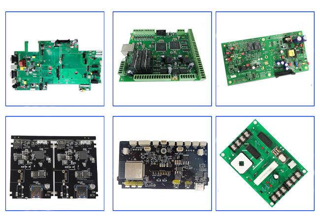
1 Layer Hdi Pcb Prototype Fast Testing Pcba Printed Circuit Board Assembly
Smart Switch Bluetooth Earphone PCBA Prototype Custom Design
Shenzhen Yideyi Technology Co., Ltd specialize in prototyping & OEM and small-volume production, making your requirment complete on the one-stop destination of boards fabrication and assembly.
EMS include consumers electronic ,medicla, industrial,power control, automotive. Temperature & Humidity ,Internet & Communication Smart Home Security etc device .
---In order to provide you with the most efficient and exactly quote on manufacturing the requested unit, we
ask that you provide us with the following information:
* Gerber file,PCB file,Eagle file or CAD file are all acceptable
* A detailed bill of materials (BOM)
* Clear pictures of PCB or PCBA sample for us
* Quantity and delivery required
* Test method for PCBA to guarantee 100% good quality products.
* Schematics file for PCB design if need to do function test.
* A sample if available for better sourcing
* A complete wiring and assembly drawing showing any special assembly instructions if required
PCBA Capability
| Board Type | Rigid, Flexible, Rigid-flexible |
| Base Material | FR4, High TG FR4, CEM1,CEM3,Aluminum, Rogers, Taconic |
| Max Board Size | 1200*400mm |
| Min Hole Size (mechanical) | 0.15mm |
| Min Hole Size (laser) | 0.10mm |
| Controlled Tolerance | +/-5% |
| Copper Weight | 0.5-4oz |
| Outline Profile | Rout/ V-cut/ Bridge/ Stamp hole |
| Solder Mask | Double-sided green LPI,Also support Red,White,Yellow,Blue,Black |
| Silk Screen | Double-sided or single-sided in white,yellow,black,or negative |
| Surface Finish | HASL, HASL lead free, Immersion Gold, Immersion Tin, Immersion Silver, Hard gold, Flash gold, OSP |
YDYA with most comprehensive ability of one-stop pcb manufacturing, pcb assembly, components sourcing in china, who has rich experience cooperating with customers among communication pcba, smart home pcba, industrial pcba, medical pcba, automotive pcba, military pcba and aerospace pcba based on certificates of ISO9001, ISO13485, ISO14000 and IATF16949
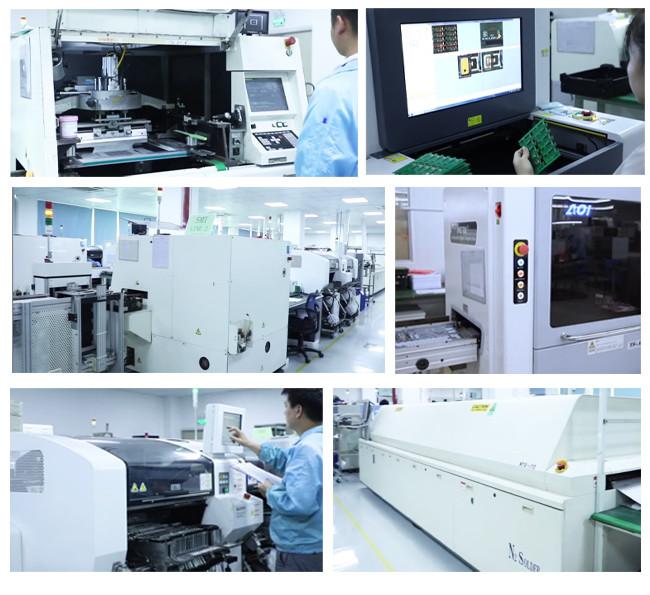
Quality comes from details control, YDY has strict quality management system, 9 steps pcb testing, ERP online monitoring, high quality pcb raw material and components ensure 99.8% pcb pass rate; precise and accurate equipments ensure 100% punctual pcba delivery.
FAQ:
Q1. How to you make the impedance calculation?
The impedance control system is done using some test coupons, the SI6000 soft and the CITS 500s equipment from POLAR INSTRUMENTS.
The equipment measures the impedance on a representative track configuration coupon of which the client has given us a determinate value and tolerance.
Q2. What kind of PCB file format can you accept for production?
Gerber, PROTEL 99SE, PROTEL DXP, CAM350, ODB+(.TGZ)
Q3. How do we ensure quality?
Our high quality standard is achieved with the following.
1. The process is strictly controlled under ISO 9001:2008 standards.
2. Extensive use of software in managing the production process
3. State-of-art testing equipments and tools. E.g. Flying Probe, X-ray Inspection, AOI (Automated Optical Inspector) and ICT (in-circuit testing).
4. Dedicated quality assurance team with failure case analysis process
5. Continuous staff training and education
Q4. How can we guarantee you receive an good quality product?
For PCB, we will use Flying Probe Test, E-test etc. for it.
For PCBA, we need you to offer us a method or test fixture for the function test.Before that, our inspectors will use microscope and X-ray to check the IC footwelding or bad solder etc.
Q5. What’s the key equipments for HDI manufacturing?
Key equipment list is as following: Laser drilling machine, Pressing machine, VCP line, Automatic Exposing machine, LDI and etc.
Q6. What’s the typical process flow for multi-layer PCB?
Material cutting → Inner dry film → inner etching → Inner AOI → Multi-bond→ Layer stack up Pressing → Drilling → PTH → Panel Plating → Outer Dry Film → Pattern Plating → Outer etching → Outer AOI → Solder Mask → Component Mark → Surface finish → Routing → E/T → Visual Inspection.
Get in Touch
Have questions about our products or want to discuss a custom order? Our team is ready to help you.