
0.2oz Diy Double Sided Pcb Fabrication Smt Electronics Manufacturing
0.2oz Double Sided PCB Assembly PCB File Or Gerber File Needed
Services we have :
* Automotive Pcb Assembly
* 2 Sided PCB Assembly
* Pcb Soldering Service
* Implementation of the firmware, IT management and programming.
* Mechanical design,including design realization and 3D models.
* Managing the documentation related to the finalization of the project.
PCB capability:
| Item | Specification | |
| 1 | Numbr of Layer | 1-16 Layers (standard) |
| 2 | Material | FR4, Aluminum, FPC |
| 3 | Surface Finish | HASL(LF), Gold plating, Enig,Immersion gold, Immersion Tin, OSP |
| 4 | Finish Board Thickness | 0.2mm-6.00 mm(8mil-126mil) |
| 5 | Copper Thickness | 1/2 oz min;12 oz max |
| 6 | Solder Mask | Green/Black/White/Red/Blue/Yellow |
| 7 | Min.Trace Width & Line Spacing | 0.075mm/0.1mm(3mil/4mil) |
| 8 | Min.Hole Diameter for CNC Driling | 0.1mm(4mil) |
| 9 | Min.Hole Diameter for punching | 0.9mm(35mil) |
| 10 | Biggest panel size | 610mm*508mm |
| 11 | Hole Positon | +/-0.075mm(3mil) CNC Driling |
| 12 | Conductor Width(W) | 0.05mm(2mil)or;+/-20% of original artwork |
| 13 | Hole Diameter(H) | PTH L:+/-0.075mm(3mil);Non-PTH L:+/-0.05mm(2mil) |
| 14 | Outline Tolerance | 0.125mm(5mil) CNC Routing;+/-0.15mm(6mil) by Punching |
| 15 | Warp & Twist | 0.70% |
| 16 | Insulation Resistance | 10Kohm-20Mohm |
| 17 | Conductivity | <50ohm |
| 18 | Test Voltage | 10-300V |
| 19 | Panel Size | 110×100mm(min);660×600mm(max) |
| 20 | Layer-layer misregistration | 4 layers:0.15mm(6mil)max;6 layers:0.25mm(10mil)max |
| 21 | Min.spacing between hole edge to circuity pattern of an inner layer | 0.25mm(10mil) |
| 22 | Min.spacing between board ouline to circuitry pattern of an inner layer | 0.25mm(10mil) |
| 23 | Board thickness tolerance | 4 layers:+/-0.13mm(5mil);6 layers:+/-0.15mm(6mil) |
| 24 | Impedance Control | +/-10% |
| 25 | Different Impendance | +-/10% |
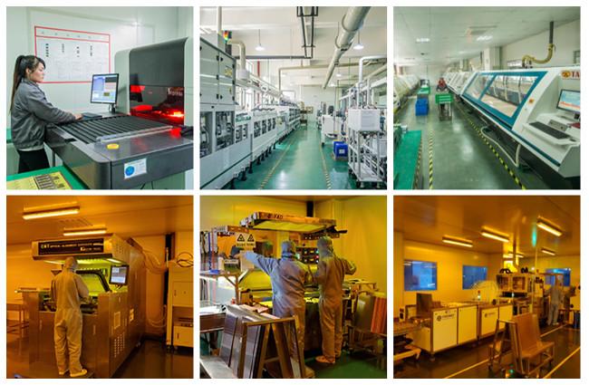
Double Sided PCB Assembly
To populate the underside with surface mount components, the PCB is inverted and the pasting and component placement process simply repeated. The second pass through the reflow oven does not melt the previously soldered side, as the joints are protected from the direct heat by being on the underside of the assembly.
This method is very common, and almost all surface mount components are specified to withstand maximum reflow temperatures with two passes through the reflow oven. Further passes through any other soldering process may compromise the components reliability.
Work with our team of 3D printing and design experts to reinvent the way you produce jigs and fixtures, rapid prototypes, tooling, on-demand parts and low-volume production runs. Our powerful 3D printing technology that produces highly accurate and durable parts that are capable of being used directly in end-use.
FAQ:
Q1. How can we ensure our information should not let third party to see our design?
We are willing to sign NDA effect by customer side local law and promising to keep customers date in high confidential level in all projects.
Q2. What service do you have?
We provide turnkey solution including RD, PCB fabrication, SMT, final assembly,testing and other value-added service.
Q3. Please note that the following detail will speed up evaluation:
Material:
Board thickness:
Copper thickness:Surface finish:
Solder mask color:
Silkscreen color:
Q4. How about your factory production capacity?
we can provide 30000 square meter/month.
Q5. With payment terms do we accept?
For sample order or small batch, we suggest you to use Pay-pal and Western Union.For mass production batch, we suggest you to use T/T.
Q6. How can we guarantee you receive an good quality product?
For PCB, we will use Flying Probe Test, E-test etc. for it.
For PCBA, we need you to offer us a method or test fixture for the function test.Before that, our inspectors will use microscope and X-ray to check the IC footwelding or bad solder etc.
Q7. What are the main products of your PCB/PCBA service?
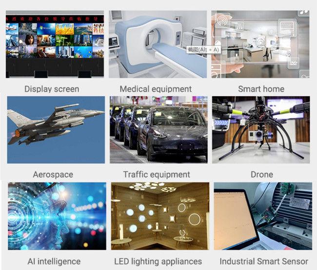
Automotive, medical, Industrial control, Internet of Things, Smart home, military, Aerospace.
Get in Touch
Have questions about our products or want to discuss a custom order? Our team is ready to help you.