
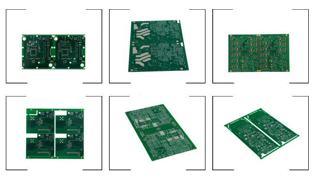
Multi Layer HDI PCB Board Design Surface Laminar Circuit PCB Stuffing
HDI PCB Board Multi-Layer Printed Circuit Boards Surface Laminar Circuit
PCB Manufacture Capacity
| Feature | Capability |
| Service Type |
HDI PCB Board Multi-Layer Printed Circuit Boards Surface Laminar Circuit |
| Quality Grade | Standard IPC 2 |
| Number of Layers | 4 - 48ayers |
| Order Quantity | 1pc - 10000+pcs |
| Build Time | 2days - 5weeks |
| Material | FR4 standard Tg 140°C,FR4 High Tg 170°C, FR4 and Rogers combined lamination |
| Board Size | Min 6*6mm | Max 457*610mm |
| Board Thickness | 0.4mm - 3.0mm |
| Copper Weight (Finished) | 0.5oz - 2.0oz |
| Min Tracing/Spacing | 2.5mil/2.5mil |
| Solder Mask Sides | As per the file |
| Solder Mask Color | Green, White, Blue, Black, Red, Yellow |
| Silkscreen Sides | As per the file |
| Silkscreen Color | White, Black, Yellow |
| Surface Finish | HASL - Hot Air Solder Leveling Lead Free HASL - RoHS ENIG - Electroless Nickle/Immersion Gold - RoHS Immersion Silver - RoHS Immersion Tin - RoHS OSP - Organic Solderability Preservatives - RoHS |
| Min Annular Ring | 4mil, 3mil - laser drill |
| Min Drilling Hole Diameter | 6mil, 4mil - laser drill |
| Max Exponents of Blind/Buried Vias | stacked vias for 3 layers interconnected, staggered vias for 4 layers interconnected |
| Other Techniques | Flex-rigid combination Via In Pad Buried Capacitor (only for Prototype PCB total area ≤1m²) |
What is HDI technology?
HDI Boards – High Density Interconnect. HDI boards, one of the fastest growing technologies in PCBs, are now available at Epec. HDI Boards contain blind and/or buried vias and often contain microvias of . 006 or less in diameter. They have a higher circuitry density than traditional circuit boards.
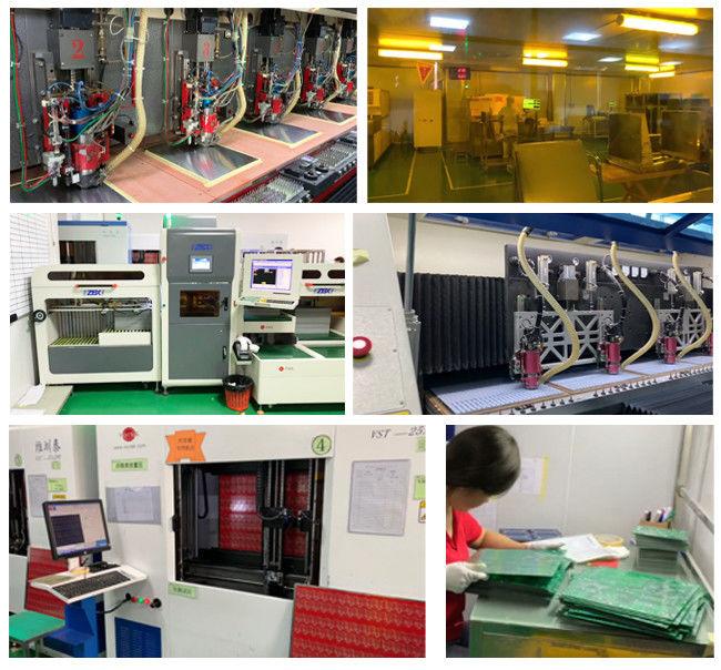
Shenzhen Yideyi Technology Co., Ltd was established in 2019, we focus on the manufacturing and development of single-layer, double-layer and multi-layer printed circuit boards.With application in the fields of telecommunications, medical equipment, computers, automobiles, and textile machine ect.
FAQs:
1, Do you offer quick turn PCB Assembly ?
Yes, we offer 24 hours quick turn PCB Assembled Solution without sacrifice the quality of the PCB Board.
2, Do you offer X-Ray capability ?
Yes, we inspect the boards using X-ray and therefore offer total reliability.
3, Do you offer conformal coating service ?
Yes, conformal coating is a part of our value-added services.
4, Do you offer testing service ?
Yes, we offer robust functional testing that adds to the product reliability.
5, Do you offer IPC 610 or J-STD Quality inspections ?
Absolutely, we offer these inspections as per client requirements.
6, Do you offer first article inspection ?
Yes, basis client requirements, we are well equipped to offer first article inspection.
7, What is your standard turnatound time for PCB Assembly ?
Our standard turnaround time for PCB Assembly is 3 weeks.
Get in Touch
Have questions about our products or want to discuss a custom order? Our team is ready to help you.