
Wireless BLE232SA-A BLUENRG 2 ST Module 8dBm BLE Mesh Module

Low-Power Bluetooth Module Low Cost Wireless Ble232SA-A St Bluenrg-2 wireless Module
|
Parameter
|
Min
|
Typ
|
Max
|
Unit
|
|
|
Operation Voltage
|
1.7
|
-
|
3.6
|
V
|
|
|
Operation Temperature
|
-30
|
-
|
85
|
°C
|
|
|
Current Consumption
|
Rest
|
-
|
5
|
-
|
mA
|
|
Standby
|
-
|
500
|
-
|
mA
|
|
|
Transmit Mode (8dBm)
|
-
|
15.1
|
-
|
mA
|
|
|
TX Power
|
-
|
-
|
8
|
dBm
|
|
|
RX Sensitivity
|
-
|
-
|
-88
|
dBm
|
|
Low-Power Bluetooth Module Low-Cost Wireless Ble232SA-A St Bluenrg-2 wireless Module
Description
BLE232SA/UA series module is designed based on ST company's BlueNRG-2. The BlueNRG-2 is a very low power Bluetooth low energy (BLE5.0)single-mode system-on-chip compliant with Bluetooth specification.
The BlueNRG-2 extends the features of the award-winning BlueNRG network processor, enabling the usage of embedded Cortex M0 for running user application code.
The BlueNRG-2 includes 256kB of programming Flash memory, 24 kB of static RAM memory with retention (two 12kB banks) and SPI, UART, I2C standard communication interface peripherals. It also features multifunction timers, watchdog, RTC and DMA controller.
An ADC is available for interfacing with analog sensors, and for reading the measurement of the integrated battery monitor. A digital filter is available for processing PDM stream.
The BlueNRG-2 offers the same excellent RF performance as the BlueNRG radio, and the integrated high-efficiency DC/DC converter keeps the same ultra-low power characteristics, but the BlueNRG-2 improves the BlueNRG sleep mode current consumption allowing a further increase in the battery lifetime of the applications.
Applications
- Watches
- Fitness, wellness and sports
- Consumer medical
- Security/proximity
- Remote control
- Home and industrial automation
- Assisted living
- Mobile phone peripherals
- Lighting PC peripher
Features
- Bluetooth low energy single mode system-on-chip compliant with Bluetooth 5.0 specifications:
master, slave and multiple simultaneous roles
LE data packet length extension
- Operating supply voltage: from 1.7 to 3.6 V
- Integrated linear regulator and DC-DC step-down converter
- Operating temperature range:
-30 °C to 85 °C
- High-performance,ultra-low-power Cortex- M0 32-bit based architecture core
- Programmable 256 kB Flash
- 24 kB RAM with retention (two 12 kB banks)
- 1 x UART interface
- 1 x SPI interface
- 2 x I²C interface
- 15GPIOs
- 2 x multifunction timer
- 10-bit ADC
- Watchdog and RTC
- DMA controller
- PDM stream processor
- 32 MHz crystal oscillator
- 32 kHz crystal oscillator
- Battery voltage monitor and temperature sensor
(at antenna connector)
- Excellent RF link budget (up to 96 dB)
- Accurate RSSI to allow power control
8.3 mA TX current (@ -2 dBm, 3.0 V)
- Down to 1 µA current consumption with active BLE stack (sleep mode)
- Average advertisement current consumption
15.34 µA (advertisement interval 1000 ms), 1 year, 8 months, 19 days with 230 mAh battery(CR2032)
- Average connection current consumption
7.059 µA (connection interval 1000 ms), 3 years, 10 months, 12 days with 230mAhbattery(CR2032)
- Suitable for building applications compliant with the following radio frequency regulations: ETSI EN 300 328, EN 300 440, FCC CFR47 part 15, ARIB STD-T66
- Pre-programmed bootloader via UART
- Up to +8 dBm available output power
Note A: ll features of BLE5.0 are not currently supported,But it is the most cost-performance chip in support of BLE5.0.
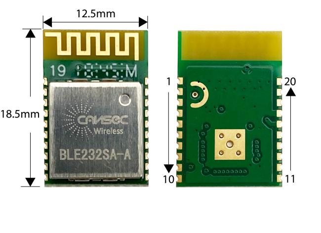
| Pad Numbe |
Name |
Pin Type |
Description |
| 1 | RESET_N | I | System reset |
|
2 |
DIO13 |
OD | GPI 13 |
| I | UART_CTS | ||
| I/O | I2C1_DAT | ||
|
3 |
DIO12 |
OD | GPI 12 |
| I/O | I2C1_CLK | ||
| 4 | GND | Ground Pin | Connect to GND |
| 5 | VCC | POWER | Battery voltage input |
|
6 |
DIO11 |
I/O | General-purpose digital I/O |
| I | UART_RXD | ||
| I/O | SPI_CS1 | ||
| O | CLK_32K | ||
|
7 |
DIO10 |
I/O | General-purpose digital I/O |
| I | SWDIO | ||
| O | SPI_OUT | ||
| O | CLK_32K | ||
|
8 |
DIO9 |
I/O | General-purpose digital I/O |
| I | SWCLK | ||
| I | SPI_IN | ||
| O | XO16/32M | ||
|
9 |
DIO8 |
I/O | General-purpose digital I/O |
| O | UART_TXD | ||
| I/O | SPI_CLK | ||
| I | PDM_DATA |
|
10 |
DIO7/BOOT |
I/O |
Bootloader pin/ General purpose digital |
| I | UART_CTS | ||
| I/O | I2C2_DAT | ||
| O | PDM_CLK | ||
|
11 |
DIO6 |
I/O | General purpose digital I/O |
| O | UART_RTS | ||
| I/O | I2C2_CLK | ||
| I | PDM_DATA | ||
|
12 |
DIO5 |
I/O | General purpose digital I/O |
| O | UART_TXD | ||
| I/O | I2C2_DAT | ||
| O | PWM1 | ||
|
13 |
DIO4 |
I/O | General purpose digital I/O |
| I | UART_RXD | ||
| I/O | I2C2_CLK | ||
| O | PWM0 | ||
|
14 |
DIO3 |
I/O | General purpose digital I/O |
| O | PWM1 | ||
| I | SPI_IN | ||
|
15 |
DIO2 |
I/O | General purpose digital I/O |
| O | PWM0 | ||
| O | SPI_OUT | ||
| O | PDM_CLK | ||
|
16 |
DIO1 |
I/O | General purpose digital I/O |
| O | UART_RTS | ||
| I/O | SPI_CS1 | ||
| I | PDM_DATA | ||
|
17 |
DIO0 |
I/O | General purpose digital I/O |
| I | UART_CTS | ||
| I/O | SPI_CLK | ||
| O | CPUCLK | ||
|
18 |
ANATEST0/DIO14 |
I/O | Analog output/ General purpose digital |
| I/O | I2C1_CLK | ||
| I/O | SPI_CLK | ||
| 19 | ADC1 | I | ADC input 1 |
| 20 | ADC2 | I | ADC input 2 |


Q1: Are you a factory or trade company?
A1: We are a professional factory with 25 years experience.
Q2: Can you accept OEM/ODM?
A2: Sure, we have rich OEM&ODM experience.
Q3: Do you have quality assurance?
A3; Each of our products has undergone quality testing and has two years of free after-sales service.
Get in Touch
Have questions about our products or want to discuss a custom order? Our team is ready to help you.