
High Purity Alumina Ceramic with Volume Resistivity of 10 4 Ohm*cm for Semiconductor Applications
High Purity Alumina Ceramic with Volume Resistivity of 10 4 Ohm*cm for Semiconductor Applications
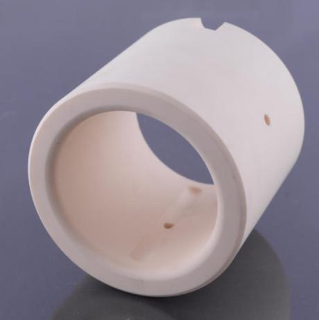
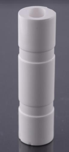
This series of semiconductor-specific alumina ceramic components are manufactured using 99.6% ultra-high purity Al₂O₃ material through precision tape casting and high-temperature sintering processes. The products exhibit excellent insulation, corrosion resistance, and dimensional stability, meeting SEMI Standard F47 cleanliness requirements.
Primary Semiconductor Applications
-
Wafer fabrication: Etching machine ceramic parts, diffusion boats
-
Packaging & testing: Probe card substrates, test sockets
-
Equipment components: Robot end effectors
-
Vacuum systems: Electrostatic chuck bases
-
Optical inspection: Lithography machine ceramic guides
Product Advantages
✓ Ultra-clean: Metal ion content <0.1ppm
✓ Precision dimensions: Tolerance ±0.05mm/100mm
✓ Plasma resistance: Etching rate <0.1μm/h
✓ Low outgassing: TML<0.1% CVCM<0.01%
✓ High reliability: Passes 1000 thermal cycles
Technical Specifications
| Parameter | Specification | Test Standard |
|---|---|---|
| Material Purity | Al₂O₃≥99.6% | GDMS |
| Volume Resistivity | >10¹⁴Ω·cm | ASTM D257 |
| Dielectric Constant | 9.8@1MHz | IEC 60250 |
| Flexural Strength | ≥400MPa | ISO 14704 |
| CTE | 7.2×10⁻⁶/°C | DIN 51045 |
| Surface Roughness | Ra≤0.1μm | ISO 4287 |
| Outgassing | TML<0.1% | ASTM E595 |
Semiconductor Manufacturing Process
-
Material preparation:
-
Nano-grade Al₂O₃ powder (D50≤0.5μm)
-
High-purity ball milling (Y₂O₃-MgO sintering aids)
-
-
Forming process:
-
Tape casting (thickness 0.1-5mm)
-
Isostatic pressing (200MPa)
-
-
Sintering control:
-
Multi-stage atmosphere sintering (1600°C/H₂)
-
HIP post-treatment (1500°C/150MPa)
-
-
Precision machining:
-
Laser processing (±5μm)
-
Ultrasonic drilling (aspect ratio 10:1)
-
-
Cleaning & inspection:
-
Megasonic cleaning (Class 1 cleanroom)
-
SEMI F47 particle testing
-
Usage Guidelines
⚠️ Storage: Class 100 clean packaging
⚠️ Installation environment: 23±1°C RH45±5%
⚠️ Cleaning: Semiconductor-grade solvents only
⚠️ Handling: Avoid direct contact with functional surfaces
Semiconductor Services
-
Cleanliness verification: VDA19 test reports
-
Failure analysis: SEM/EDS microanalysis
-
Custom development: DFM co-design
FAQ
Q: How to ensure wafer contact surface cleanliness?
A: Triple protection:
① Plasma surface activation
② Vacuum packaging + N₂ storage
③ Pre-installation ionized air cleaning
Q: Performance in fluorine-based plasma?
A: Special treated version:
• Etching rate <0.05μm/h
• AlF₃ passivation layer
• 3x longer lifespan
Q: Maximum processable size?
A: Standard 200×200mm, special process up to 400×400mm.


Get in Touch
Have questions about our products or want to discuss a custom order? Our team is ready to help you.