
Customizable Board Thinkness PCB FR4 Multilayer Design HASL Treatment
Customized FR4 Multilayer Layer PCB
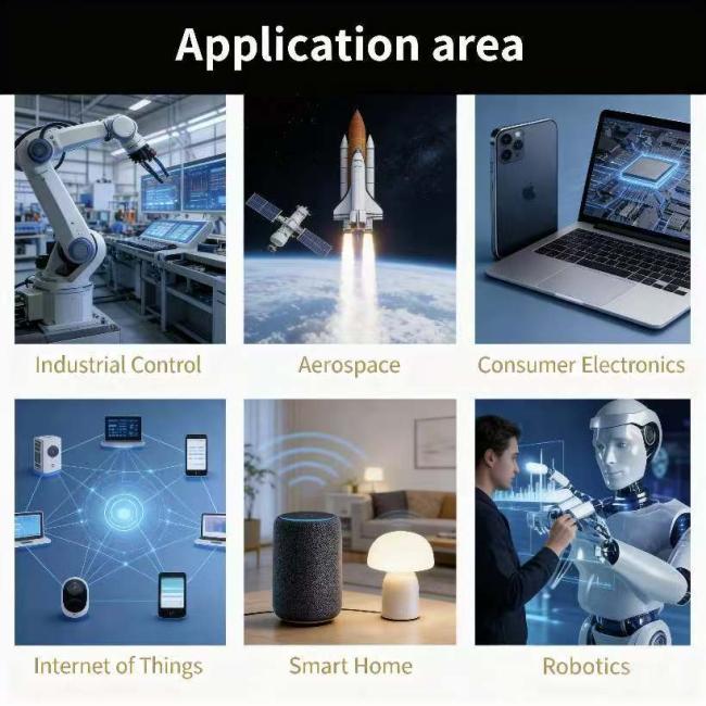
This high-performance multilayer PCB is expertly engineered to deliver exceptional electromagnetic compatibility (EMC), significantly reduced signal crosstalk, and improved signal integrity. Its multi-layer structure with premium dielectric materials isolates sensitive signal paths, ensuring stable high-frequency transmission. Ideal for advanced electronics: high-efficiency power supplies, 5G communication modules, rugged industrial controls, and compact embedded systems, meeting stringent technical demands for reliability and precision.
Advantages of Multilayer PCB:
- Increase circuit board density
- Reduce size
- Better signal integrity
- Adapt to high-frequency applications
- Better thermal management
- Higher reliability
Basical Features:
- Multi-layer design
- Inner layer and outer layer
- through hole
- Copper layer
- Dielectric layer (dielectric material)
Multilayer PCB Customized services:
Send us your:
1. Gerber files (RS-274X)
2. BOM (if PCBA needed)
3. Impedance requirements & stack-up (if available)
4.Test requirements (TDR, network analyzer, etc.)
Tips:Normally,Gerber files includes: PCB type,thickness, ink color, surface treatment process, and if SMT processing is required, you can provide a component BOM and reference designation diagram, etc.
We’ll reply within 24 hours with a free quote, DFM report, and material recommendation.
Manufacturing process:
- Design and layout: During the design phase, engineers use PCB design software to lay out and route multilayer circuit boards, determining the functions of each's circuit and the interconnection method between layers.
- Lamination: During the manufacturing process, multiple circuit layers are pressed together through a lamination process, with each layer separated by an insulating material. lamination process is typically carried out under high temperature and high pressure conditions.
- Drilling and electroplating: Through-hole connections between different layers of the circuit are formed by drilling technology, and then electroplating is carried out ensure the conductivity of the through-holes.
- Assembly and welding: After the components are installed, they can be soldered and connected using surface-mount technology (SMT) or traditional through-hole technologyTHT).

Factory showcase

PCB Quality Testing

Certificates and Honors

Get in Touch
Have questions about our products or want to discuss a custom order? Our team is ready to help you.