
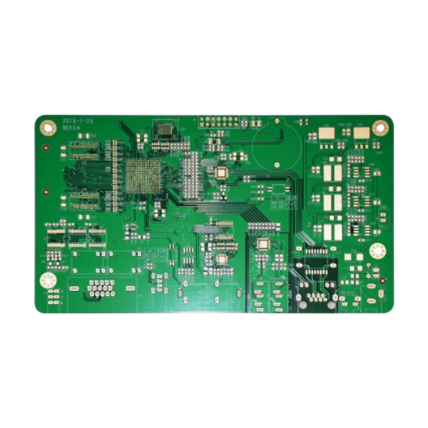
High Quality Mobile Phone PCB Production
Price:
Contact us
MOQ:
1
Delivery Time:
Negotiable
Product Description
High Quality Mobile Phone PCB Production
What's Mobile Phone PCB Production?
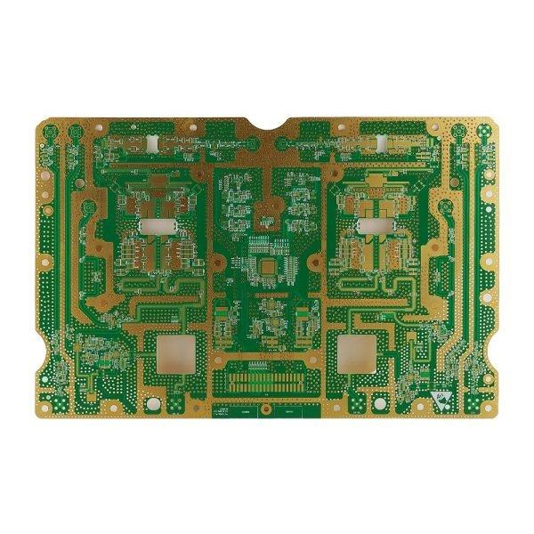
Mobile Phone PCB Production is the process of designing and fabricating the printed circuit boards (PCBs) that serve as the backbone of smartphones. It involves several key stages:
- Design & Layout: Engineers use specialized software to create a multi-layer schematic that positions components like the processor, memory, and antennas for optimal performance and minimal space usage.
- Material Selection: High-performance substrates (e.g., FR-4, polyimide, or advanced low-loss laminates) are chosen based on electrical, thermal, and mechanical requirements, especially for 5G and high-speed signals.
- Fabrication:
- A copper-clad laminate is drilled and etched to form fine traces and vias.
- Multiple layers are stacked and bonded to create a compact multilayer board.
- Surface finishes (ENIG, OSP, etc.) are applied to protect copper and enable soldering.
- Assembly: Surface-Mount Technology (SMT) places and solders tiny components; through-hole parts are added if needed. Automated optical and X-ray inspections ensure joint quality.
- Testing & Integration: Electrical tests, signal-integrity checks, and thermal cycling verify reliability before the PCB is integrated into the phone chassis.
Technical Parameters
| Item | Specification |
|---|---|
| Layers | 1~64 |
| Board thickness | 0.1mm-10.0mm |
| Material | FR-4, CEM-1/CEM-3, PI, High Tg, Rogers |
| Max panel size | 32"×48"(800mm×1200mm) |
| Min hole size | 0.075mm |
| Min line width | 3mil(0.075mm) |
| Surface finish | OSP, HASL, Imm Gold/Nickel/Ag, Electric gold |
| Copper thickness | 0.5-15 OZ |
| Soldermask | Green/Yellow/Black/White/Red/Blue |
| Silkscreen | Red/Yellow/Black/White |
| Min PAD | 5mil(0.13mm) |
| Inter package | Vacuum |
| Outer package | Carton |
| Outline tolerance | ±0.75mm |
| Hole tolerance | PTH:±0.05 NPTH:±0.025 |
| Certificate | UL, ISO 9001, ISO14001, IATF16949 |
| Special request | Blind hole+Gold finger + BGA |
| Material Suppliers | Shengyi, KB, Nanya, ITEQ, etc. |
One-Stop PCBs Solution


Advantages of DQS Team
On-time Delivery:
- Owned PCBA factories 15,000 ㎡
- 13 fully automatic SMT lines
- 4 DIP assembly lines
Quality Guaranteed:
- IATF, ISO, IPC, UL standards
- Online SPI, AOI, X-Ray Inspection
- The qualified rate of products reach 99.9%
Premium Service:
- 24H reply your inquiry
- Perfect after-sales service system
- From prototype to mass production
Similar Products
Get in Touch
Have questions about our products or want to discuss a custom order? Our team is ready to help you.
Company
DQS Electronic Co., Limited
Location
Yasen Industrial Park, Baolong Street, Longgang District, Shenzhen
Contact Person
Jason Guan