
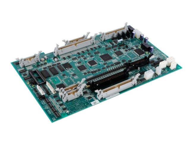
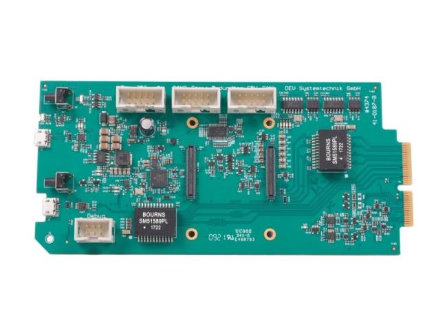
LED Light SMT PCB Board Aluminum Electronic Multilayer PCBA
Price:
Negotiable
MOQ:
1
Delivery Time:
5-30 word days
Product Description
LED Light SMT PCB Board Aluminum Electronic Multilayer PCBA
LED Light SMT PCB Board Aluminum Electronic Multilayer PCBA
What is multilayer PCBA?
Multilayer PCBA (Multilayer Printed Circuit Board Assembly) is the fully assembled board that contains three or more conductive copper layers laminated together with insulating dielectric material. These internal layers are interconnected by plated-through, blind or buried vias, and carry traces, power planes and ground planes. After the bare multilayer PCB is fabricated, electronic components (both SMD and THT) are soldered onto its outer surfaces, creating the functional multilayer PCBA.
Key points:
-
Structure
- Alternating layers of copper foil and prepreg/core are pressed into one rigid board.
- Inner layers are etched beforehand; outer layers receive components and final plating.
- Vias (through, blind, buried) provide layer-to-layer connectivity without enlarging the board.
-
Assembly flow
- Identical to standard PCBA: solder-paste printing -> pick-and-place -> reflow (and/or wave) soldering -> AOI/X-ray/ICT -> final test.
- Extra precautions for warpage and via reliability because of the thicker, high-layer-count substrate.
-
Design advantages
- Dense, high-speed or RF circuits with dedicated power/ground planes for low noise.
- Miniaturization--more circuitry per cm², essential for smartphones, wearables, aerospace, medical implants, etc.
- Controlled impedance, better EMI shielding and thermal management compared with single- or double-sided boards.
-
Typical layer counts
- Consumer products: 4-12 layers.
- High-end servers, telecom, military: 20-60 layers.
- Specialty suppliers can exceed 100 layers, but cost and yield become critical.
Technical Parameters
| PCB Assembly Capability | ||
|---|---|---|
| Item | Normal | Special |
| SMT Assembly | PCB(used for SMT) specification | |
| Length and Width( L* W) | Minimum: L≥3mm, W≥3mm Maximum: L≤800mm, W≤460mm |
L<2mm L>1200mm, W>500mm |
| Thickness( T) | Thinnest: 0.2mm Thickest: 4 mm |
T<0.1mm T>4.5mm |
| SMT components specification | Outline Dimension Min size: 0201(0.6mm*0.3mm) Max size: 200 * 125 component thickness: T≤15mm |
01005(0.3mm*0.2mm) 200 * 125 6.5mm<T≤15mm |
| QFP,SOP,SOJ (multi pins) | Min pin space: 0.4mm | 0.3mm≤Pitch<0.4mm |
| CSP/ BGA | Min ball space: 0.5mm | 0.3mm≤Pitch<0.5mm |
| DIP Assembly | PCB specification | |
| Length and Width( L* W) | Minimum: L≥50mm, W≥30mm Maximum: L≤1200mm, W≤450mm |
L<50mm L≥1200mm, W≥500mm |
| Thickness( T) | Thinnest: 0.8mm Thickest: 3.5mm |
T<0.8mm T>2mm |
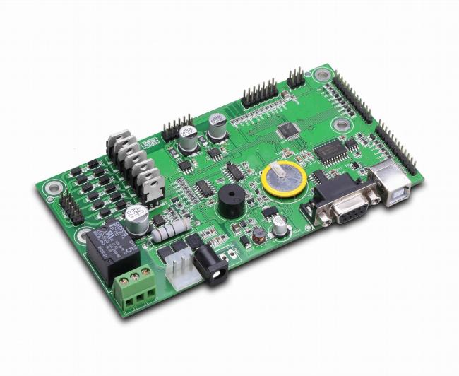
One-Stop PCBA Solution
PCBA Prototype
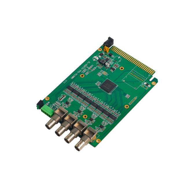
Industrial Control PCBA
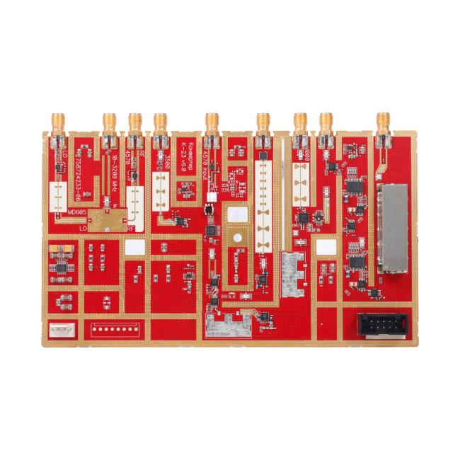
Telecom PCBA
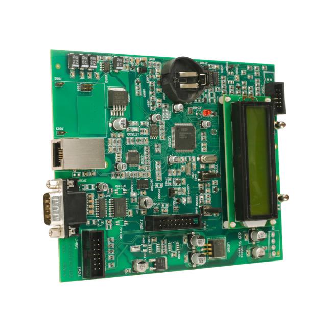
Medical PCBA
Automotive PCBA
Consumer Electronic PCBA
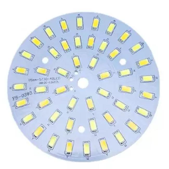
LED PCBA
Security PCBA
Advantages of DQS Team
1. On-time Delivery:
- Owned PCBA factories 15,000 ㎡
- 13 fully automatic SMT lines
- 4 DIP assembly lines
2. Quality Guaranteed:
- IATF, ISO, IPC, UL standards
- Online SPI, AOI, X-Ray Inspection
- The qualified rate of products reach 99.9%
3. Premium Service:
- 24H reply your inquiry
- Perfect after-sales service system
- From prototype to mass production
Similar Products
Get in Touch
Have questions about our products or want to discuss a custom order? Our team is ready to help you.
Company
DQS Electronic Co., Limited
Location
Yasen Industrial Park, Baolong Street, Longgang District, Shenzhen
Contact Person
Jason Guan