
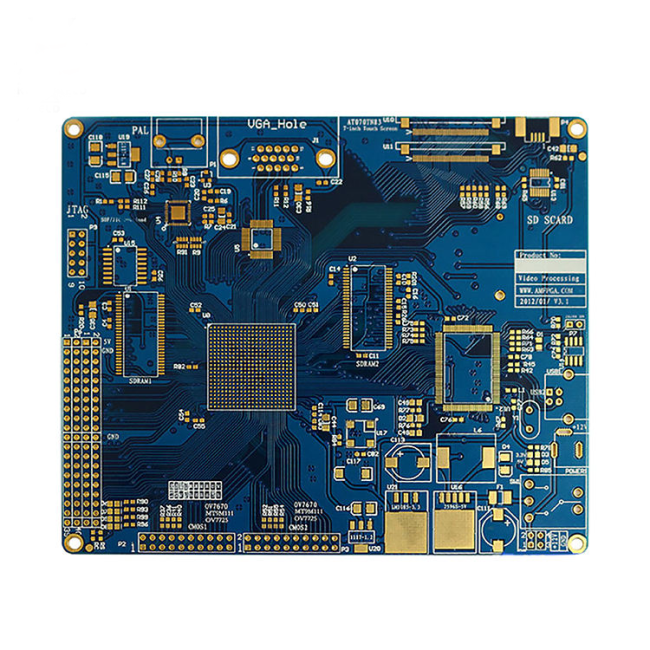
SL S1000-2M 6-layer Minimum aperture 0.3mm EPS pcb board HDI pcb boards
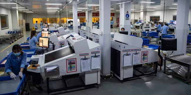
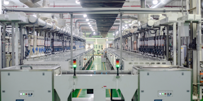
Shenzhen Hing Technology Co., Ltd was established in 2016. The company is a national high-tech enterprise specializing in the research and development, production and sales of printed circuit boards. Since its establishment, the company has long adhered to the development strategy of quality first, technology as the core, and customer demand as the orientation, focusing on the high-end segmented circuit board market covering an area of approximately 10000 square meters.
The company's products are widely used in communication, new energy, industrial control, consumer electronics, automotive electronics and medical electronics and other application fields, and the products serve well-known customers at home and abroad.
- With up to 14 layer any layer capability
- Min line width and spacing in volume production is around 40μm
- Fine pitch BGA with 0.35mm
- Capability of plated copper or filled with conductive paste for stacked microvias
- Heavy Copper, embedded coin and provide a thermal management solution
- Support planar surface for ball grid array ("BGA") (Via-in-Pad) Enhance impedance performance
- Enhance impedance performance
- Microvias solutions for Radio Frequency HDI boards
- High speed material for hybrid HDI
- Wide range laminate support (Low Tg , high Tg material and halogen free material )
- Low-DK laminate for smart devices
- Signal integrity enhancement
- Edge plating capability
-
Technical Parameter
-
o. Capabilities Standard Production Advanced Production 1 Stack up Blind/Buried/Anylayer board Lamination times MAX≤5times MAX≤6times Copper thickness Inner layer 1/3OZ-2oz
MAX 2OZ1/4OZ-2oz
MAX OZOuter layer 1/3OZ-3OZ 1/3OZ-2OZ Min Dielectric ThK 35um(1027) 30um (1017) Structure 1-N-1 / 2-N-2 / 3-N-3 1-N-1 / 2-N-2 / 3-N-3 / 4-N-4 / ELIC(12L) Layer count 4-24 4-34 2 Min. Line/Space Min L/W (inner) 2/2mil (50/50um) 1.6/1.6 mil ( 40/40um) Min. L/W (Outer) 2.4/2.4mil (60/60um) 2/2mil (50/50um) 3 Line/Space Inner Layer Tenting 2/2mil (50/50um) 1.6/1.6 mil ( 40/40um) mSAP 1.4/1.4mil (40/40um) 1.2/1.2mil (35/35um) Outer layer Tenting 3/3mil (75/75um) 2.4/2.4 mil ( 60/60um) mSAP 2.4/2.4mil (60/60um) 2/2mil (50/50um) Pad size inner layer min size 225um 200um outter layer min size 225um 200um 4 Drill min Mechanical Drill size 0.2mm 0.15mm PTH plating A/R ≤8:1 ≤10:1 PTH Hole Tolerance ±0.075mm ±0.075mm NPTH Hole Tolerance ±0.05mm ±0.05mm Plated slot tolerance Long slot ±0.075mm ±0.075mm Short Slot ±0.1mm ±0.1mm 5 Min BGA Min BGA/ BGA pitch 0.4 0.35 6 Laser Min. Laser hole size 75um 50um Min. distance from laser hole to laser hole 0.025mm 0.025mm Laser hole plating A/R ≤0.8:1 ≤1:1 7 Soldermask Color Green,Yellow,Black,Blue,Red, White, Matt green Green,Yellow,Black,Blue,Red, White, Matt green SM ThK Single print thickness 10-30um 10-30um Min SM dam 3.0mil 2.5mil 8 Impedance Capability of Impedance Single line impedance<50Ω ±3.5Ω ±3.5Ω Single line impedance≥50Ω ±10% ±7% Differential line impedance ±10% ±7% 9 Tolerance capability Patten size tolerance pad size tolerance ±20% ±15% line tolerance ±20% ±15% patten to outline +/- 0.0075mm +/- 0.0050mm Registration tolerance laser A/R 100um 75um PTH A/R 100um 75um ![]()

- Your inquiry will be replied within 12 hours
- Well-trained & experienced sales can reply your inquiries in English
- During working time, E-mail will be replied to you within 2 hours
- OEM & ODM projects are highly welcomed, we have strong R&D team
- The order will be produced exactly according to order details and proofed samples, our QC will submit inspection report before shipment
- Your business relationship with us will be confidential to any third party
- Good after-sale service
Get in Touch
Have questions about our products or want to discuss a custom order? Our team is ready to help you.