
4H-N Type SiC Substrate 10x10mm Wafer for Power Electronics
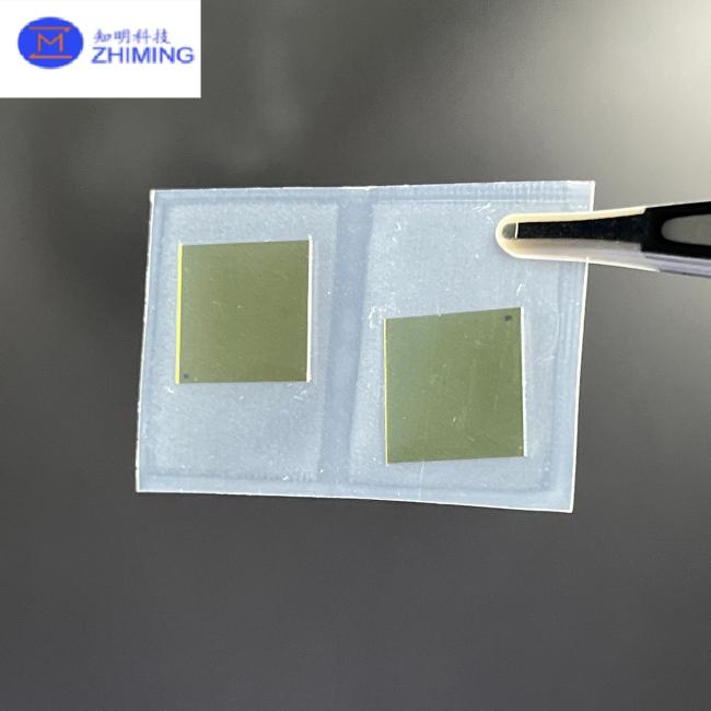
The 4H-N type SiC 10*10 mm small wafer is a high-performance semiconductor substrate based on silicon carbide (SiC), a third-generation semiconductor material. Fabricated via Physical Vapor Transport (PVT) or High-Temperature Chemical Vapor Deposition (HTCVD), it is available in 4H-SiC or 6H-SiC polytypes and N-type or P-type doping configurations. With dimensional tolerances within ±0.05 mm and surface roughness Ra < 0.5 nm, each wafer is epitaxial-ready and undergoes rigorous inspection, including XRD crystallinity validation and optical microscopy defect analysis.
| Parameter | Specification |
|---|---|
| Material Type | 4H-SiC (N-type doped) |
| Dimensions | 10*10 mm (±0.05 mm) |
| Thickness | 100–500 μm |
| Surface Roughness | Ra < 0.5 nm (polished) |
| Resistivity | 0.01–0.1 Ω·cm |
| Crystal Orientation | (0001) ±0.5° |
| Thermal Conductivity | 490 W/m·K |
| Defect Density | Micropipes: <1 cm⁻²; Dislocations: <10⁴ cm⁻² |
- High Thermal Conductivity: 490 W/m·K, three times that of silicon, enabling efficient heat dissipation.
- Breakdown Strength: 2.4 MV/cm, supporting high-voltage and high-frequency operation.
- High-Temperature Stability: Operational up to 600°C with low thermal expansion (4.0*10⁻⁶/K).
- Mechanical Durability: Vickers hardness 28–32 GPa, flexural strength >400 MPa.
- Customization Support: Adjustable orientation, thickness, doping, and geometry.
- Electric vehicle power inverters (3–5% efficiency gain)
- 5G RF power amplifiers (24–39 GHz bands)
- Smart grid HVDC converters and industrial motor drives
- Aerospace sensors and satellite power systems
- UV LEDs and laser diodes

- 4H-N SiC Substrate, 5*5 mm, 350 μm (Prime/Dummy Grade)
- Custom-shaped SiC wafers with backside metallization
Q: What are typical applications of 10*10 mm SiC wafers?
A: Ideal for prototyping power devices (MOSFETs/diodes), RF components, and high-temperature optoelectronics.
Q: How does SiC compare to silicon?
A: SiC offers 10* higher breakdown voltage, 3* better thermal conductivity, and superior high-temperature performance.
- Complete production chain from cutting to final cleaning and packing.
- Capability to reclaim wafers with diameters 4-inch—12-inch.
- 20 year experience of wafering and reclaiming of monocrystalline electronic materials
ZMSH Technology can provide customers with imported and domestic high-quality conductive, 2-6inch semi-insulating and HPSI (High Purity Semi-insulating) SiC substrates in batches; In addition, it can provide customers with homogeneous and heterogeneous silicon carbide epitaxial sheets, and can also be customized according to the specific needs of customers, with no minimum order quantity.
Get in Touch
Have questions about our products or want to discuss a custom order? Our team is ready to help you.