
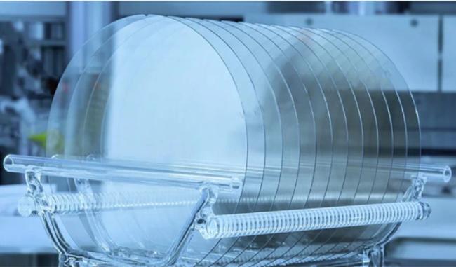
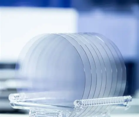
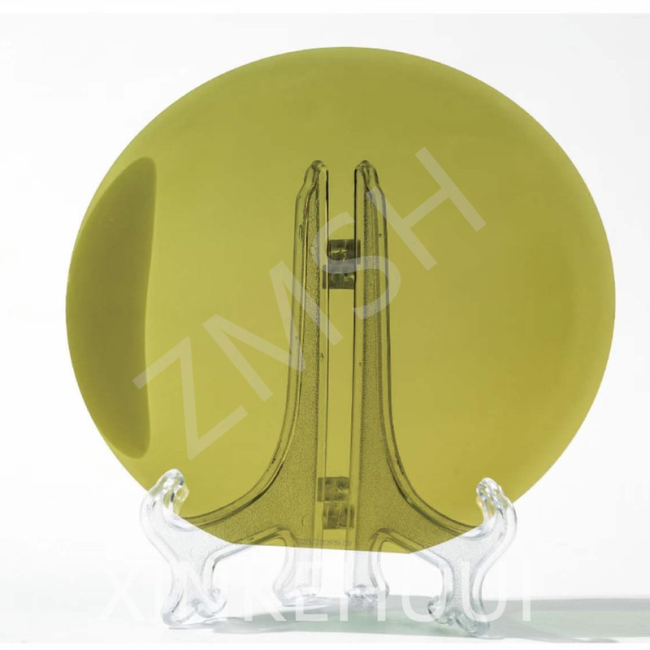
HPSI SiC Wafer 2-12 Inch Optical Grade for AI/AR Glasses
HPSI SiC Wafer Overview
HPSI SiC Wafer 2-12 Inch Optical Grade for AI/AR Glasses
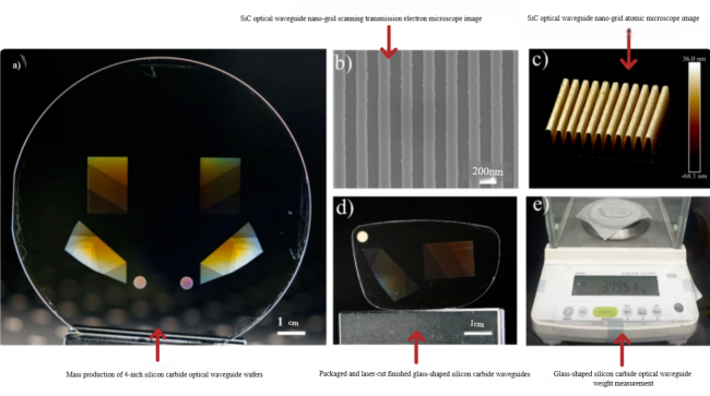
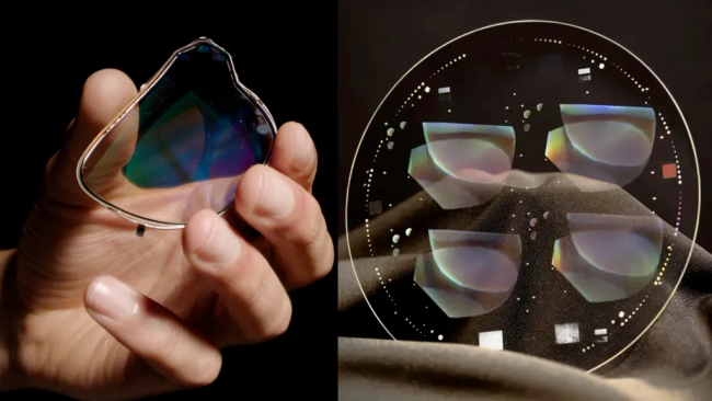
HPSI-type SiC wafers (High-Purity Semi-Insulating Silicon Carbide) serve as core optical materials in AI and AR glasses. With their high refractive index (2.6–2.7 @ 400–800 nm) and low optical absorption characteristics, they address issues like "rainbow effects" and insufficient light transmittance in traditional glass or resin materials for AR waveguides. For example, Meta’s Orion AR glasses utilize HPSI SiC waveguide lenses, achieving a 70°–80° ultra-wide field of view (FOV) with a single-layer lens thickness of only 0.55 mm and weight of 2.7 g, significantly enhancing wear comfort and immersion.
HPSI SiC Wafer Core Features & Advantages
Material Properties, Optical Performance, and Application Value
1. Refractive Index: 2.6–2.7
- This high refractive index allows replacing multi-layer optical structures with a single-layer lens, reducing light loss and enhancing brightness and color accuracy. Consequently, it enables purer visual displays, eliminates rainbow effects, and supports seamless integration with high-resolution Micro LEDs.
2. Thermal Conductivity: 490 W/m·K
- The material rapidly dissipates heat generated by high-power Micro LEDs, preventing lens deformation and extending device lifespan. This ensures stable performance even in high-temperature environments, such as outdoor use.
3. Mohs Hardness: 9.5
- With exceptional scratch resistance, the material withstands daily wear and tear. This reduces maintenance needs and extends the lens’s service life, improving long-term usability.
4. Wide Bandgap Semiconductor
- Its compatibility with CMOS processes enables nanoscale lithography and etching for precise optical grating fabrication. This facilitates wafer-scale production of advanced optical components like diffractive waveguides and micro-resonators.
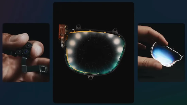
HPSI SiC Wafer Key Applications
1. AI/AR Optical Systems
- Waveguide Lenses: Triangular cross-section grating design enables single-layer full-color displays, resolving chromatic dispersion in traditional diffractive waveguides (e.g., Meta Orion solution).
- Micro-Display Couplers: Achieves >80% light transmission efficiency between Micro LEDs and waveguides.
- Anti-Reflective Coating Substrates: Minimizes environmental light reflections, enhancing AR contrast ratios.
2. Expanded Applications
- Quantum Communication Devices: Leverages color center properties for quantum light source integration.
- High-Power Laser Components: Serves as substrates for laser diodes in industrial cutting and medical systems.
HPSI SiC Wafer Key Parameter
| 4-Inch and 6-Inch Semi-Insulating SiC Substrate Specification Comparison | |||
| Parameter | Grade | 4-Inch Substrate | 6-Inch Substrate |
| Diameter | Z Grade / D Grade | 99.5 mm - 100.0 mm | 149.5 mm - 150.0 mm |
| Poly-type | Z Grade / D Grade | 4H | 4H |
| Thickness | Z Grade | 500 μm ± 15 μm | 500 μm ± 15 μm |
| D Grade | 500 μm ± 25 μm | 500 μm ± 25 μm | |
| Wafer Orientation | Z Grade / D Grade | On axis: <0001> ± 0.5° | On axis: <0001> ± 0.5° |
| Micropipe Density | Z Grade | ≤ 1 cm² | ≤ 1 cm² |
| D Grade | ≤ 15 cm² | ≤ 15 cm² | |
| Resistivity | Z Grade | ≥ 1E10 Ω·cm | ≥ 1E10 Ω·cm |
| D Grade | ≥ 1E5 Ω·cm | ≥ 1E5 Ω·cm | |
| Primary Flat Orientation | Z Grade / D Grade | (10-10) ± 5.0° | (10-10) ± 5.0° |
| Primary Flat Length | Z Grade / D Grade | 32.5 mm ± 2.0 mm | Notch |
| Secondary Flat Length | Z Grade / D Grade | 18.0 mm ± 2.0 mm | - |
| Edge Exclusion | Z Grade / D Grade | 3 mm | 3 mm |
| LTV / TTV / Bow / Warp | Z Grade | ≤ 2.5 μm / ≤ 5 μm / ≤ 15 μm / ≤ 30 μm | ≤ 2.5 μm / ≤ 6 μm / ≤ 25 μm / ≤ 35 μm |
| D Grade | ≤ 10 μm / ≤ 15 μm / ≤ 25 μm / ≤ 40 μm | ≤ 5 μm / ≤ 15 μm / ≤ 40 μm / ≤ 80 μm | |
| Roughness | Z Grade | Polish Ra ≤ 1 nm / CMP Ra ≤ 0.2 nm | Polish Ra ≤ 1 nm / CMP Ra ≤ 0.2 nm |
| D Grade | Polish Ra ≤ 1 nm / CMP Ra ≤ 0.2 nm | Polish Ra ≤ 1 nm / CMP Ra ≤ 0.5 nm | |
| Edge Cracks | D Grade | Cumulative area ≤ 0.1% | Cumulative length ≤ 20 mm, single ≤ 2 mm |
| Polytype Areas | D Grade | Cumulative area ≤ 0.3% | Cumulative area ≤ 3% |
| Visual Carbon Inclusions | Z Grade | Cumulative area ≤ 0.05% | Cumulative area ≤ 0.05% |
| D Grade | Cumulative area ≤ 0.3% | Cumulative area ≤ 3% | |
| Silicon Surface Scratches | D Grade | 5 allowed, each ≤1mm | Cumulative length ≤ 1 x diameter |
| Edge Chips | Z Grade | None permitted (width and depth ≥0.2mm) | None permitted (width and depth ≥0.2mm) |
| D Grade | 7 allowed, each ≤1mm | 7 allowed, each ≤1mm | |
| Threading Screw Dislocation | Z Grade | - | ≤ 500 cm² |
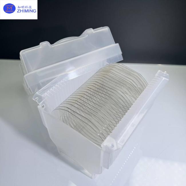
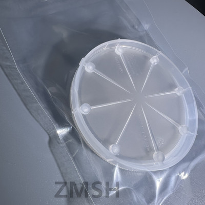
| Packaging | Z Grade / D Grade | Multi-wafer Cassette Or Single Wafer Container | Multi-wafer Cassette Or Single Wafer Container |
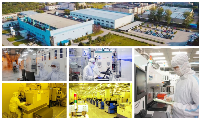
ZMSH Services
ZMSH as an integrated manufacturing and trading entity, delivers end-to-end solutions for SiC products:
-
Vertical Integration: In-house crystal growth furnaces produce 4H-N, 4H-HPSI, 6H-P, and 3C-N type wafers (2–12-inch), with customizable parameters (e.g., doping concentration, bending strength).
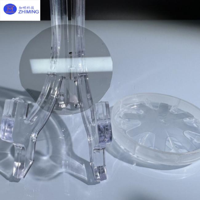
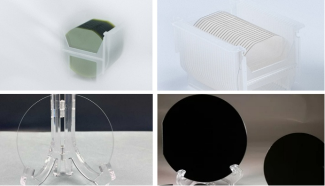
- Precision Processing:
- Wafer-Level Cutting: Laser dicing and chemical mechanical polishing (CMP) achieve surface roughness <0.3 nm.
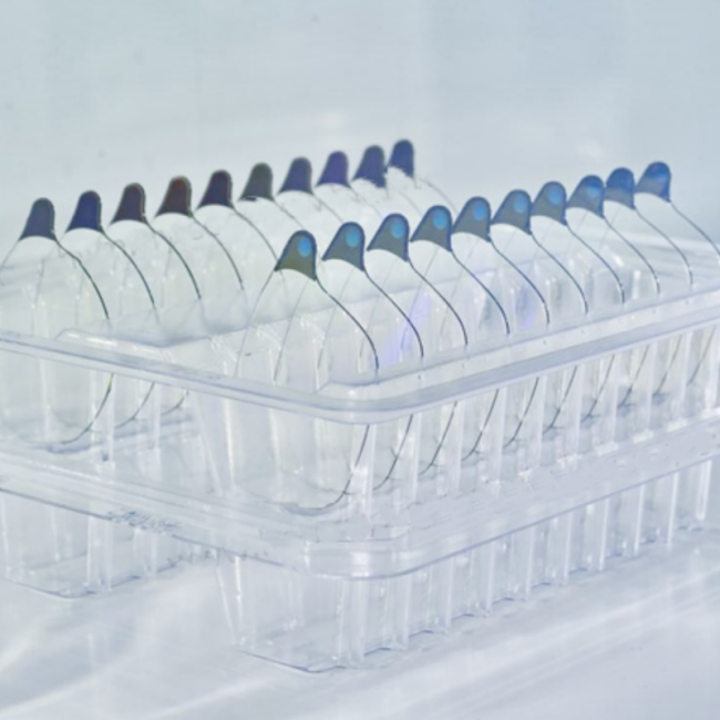
- Custom Shapes: Produces prisms, square wafers, and waveguide arrays for AR optical module integration.
- Contact Us: Samples and technical consultations available. Full-service support from design validation to mass production.
ZMSH's SiC Products
SiC Wafers 4H-Semi
SiC Wafers 4H-N
Other types of SiC samples
HPSI SiC Wafer FAQ
Q1: Why is HPSI SiC Wafer critical for AR glasses?
A1: HPSI SiC Wafer’s high refractive index (2.6–2.7) and low optical absorption eliminate rainbow effects in AR displays while enabling ultra-thin waveguides (e.g., Meta Orion’s 0.55mm lenses).
Q2: How does HPSI SiC differ from traditional glass in AR optics?
A2: HPSI SiC offers 2x higher refractive index than glass (~2.0), allowing wider FOV and single-layer waveguides, plus 490 W/m·K thermal conductivity to manage heat from Micro LEDs.
Q3: Is HPSI SiC compatible with other semiconductor materials?
A3: Yes, it integrates with GaN and silicon in hybrid systems, but its thermal stability and dielectric properties make it superior for high-power AR optics.
Tags: #HPSI SiC Wafer, #Silicon Carbide Substrate, #Customized, #Double-Side Polished, #High-Purity, #Optical Component, #Corrosion-Resistant, #High-Temperature Rated, #HPSI, #Optical-Grade, #2-12 Inch, #Optical Grade, #AI/AR Glasses
Get in Touch
Have questions about our products or want to discuss a custom order? Our team is ready to help you.