
2-Inch C-Plane Sapphire Substrate for Process Development & Equipment Calibration
2-Inch C-Plane Sapphire Substrate for Process Development & Equipment Calibration
Product Overview
This 2-inch C-plane sapphire substrate is manufactured from high-purity single-crystal aluminum oxide (Al₂O₃) using advanced crystal growth and precision slicing techniques. Featuring a Single-Side Polished (SSP) surface, stable thickness, and low bow control, this substrate is ideal for equipment calibration, thin-film deposition trials, and non-critical semiconductor or photonics R&D.
Each wafer undergoes strict dimensional and visual inspection, and all shipments include full batch traceability.
Key Features
-
High-Purity Sapphire (Al₂O₃): Excellent mechanical strength, thermal stability, and chemical resistance.
-
C-Plane (0001) Orientation: Standard orientation for GaN, optical coatings, and laser applications.
-
SSP Surface: Polished front side ensures uniform deposition; backside lapped for stable fixture handling.
-
Low Bow <10 µm: Maintains flatness for reliable processing.
-
Dummy Grade: Cost-effective for process experiments and equipment tuning.
-
Strict Quality Control: Batch No. and Lot No. provided for full traceability.
Technical Specifications
| Item | Specification |
|---|---|
| Product | 2-inch C-Plane SSP Sapphire Substrate |
| Material | Single-Crystal Al₂O₃ |
| Diameter | 50.8 mm |
| Orientation | C-plane (0001) |
| Thickness | 430 µm ± 25 µm |
| Surface Finish | SSP (Single Side Polished) |
| Bow | <10 µm |
| Grade | Dummy Grade |
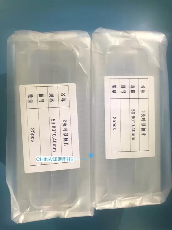
| Quantity | 25 pcs |
Applications
This dummy-grade sapphire substrate is suitable for:
-
Deposition trials (ALD / PVD / CVD / MOCVD)
-
Equipment calibration and parameter tuning
-
Coating uniformity and process evaluation
-
Thin-film R&D and non-critical photonics experiments
-
University training and laboratory teaching
-
Optical testing and functional demonstration setups
Packaging & Quality Assurance
-
Class 100 cleanroom inspection and handling
-
25 pcs per wafer cassette with protective separators
-
Vacuum-sealed, anti-static packaging to prevent contamination
-
Lot and batch labels included for full traceability
-
Visual defect screening before shipment
FAQ
1. What is the main difference between dummy-grade and prime-grade sapphire substrates?
Dummy-grade substrates have correct mechanical dimensions but may not meet the optical, surface defect, or epi-ready standards required for GaN growth or device manufacturing. They are ideal for process testing and calibration.
2. Can I use this substrate for epitaxial growth?
For general process verification, yes.
However, for high-quality GaN or epitaxial device fabrication, we recommend switching to prime-grade or epi-ready DSP sapphire for better flatness, TTV, and surface defect control.
3. Do you offer customized orientation, thickness, or polishing?
Yes. We support custom:
-
Thickness (200–1500 µm)
-
SSP / DSP
-
C-plane, A-plane, R-plane, M-plane
-
Laser marking, orientation flats, custom chamfering
Please contact us with your specifications.
Related Product
ultrathin thickness 0.1mm 0.2mm 2inch sapphire double side polished wafer
Get in Touch
Have questions about our products or want to discuss a custom order? Our team is ready to help you.