
51mm Natural Transparent Wafer Jar for Semiconductor Industry - 4" to 8" Sizes with 1.5" to 3" Height Options
Price:
5~8 USD/SET
MOQ:
50PCS(Negotiable)
Delivery Time:
20~25 Working days
Brand:
Hiner-pack
Product Description
Product Overview
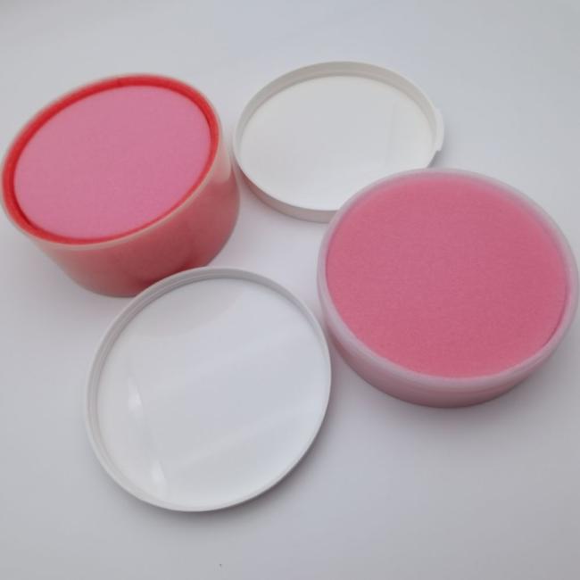
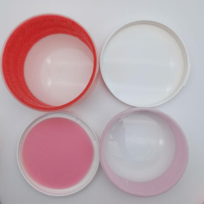
51mm natural transparent wafer jars designed specifically for semiconductor industry applications. These precision containers provide secure transportation and storage for wafers of various thicknesses with an innovative open-box design.
Key Features & Benefits
Secure Wafer Protection
Constructed from PP material with micro-elastic properties, these wafer jars work in conjunction with foam pads and liners to prevent wafer wear and scratches during transportation.
Convenient Operation
Easy-rotate design allows simple opening and closing, facilitating quick placement and retrieval of wafers for manual operations.
Cost-Effective Solution
Lightweight construction reduces loading and transportation costs while maintaining superior protection for semiconductor components.
Flexible Capacity
Customizable loading quantities with foam padding options to accommodate various sample sizes and bulk shipment requirements.
Product Specifications
| Product | Dimension | Height | Diameter | Material | Color | Surface Resistance |
|---|---|---|---|---|---|---|
| Wafer Jar | 4″ | 1.5" | 113mm | Ultra Clean PP | Transparent | N/A |
| Wafer Jar | 6″ | 2" | 163mm | Ultra Clean PP | Transparent | N/A |
| Wafer Jar | 6″ | 3" | 163mm | Ultra Clean PP | Transparent | N/A |
| Wafer Jar | 8″ | 2" | 230mm | Ultra Clean PP | Transparent | N/A |
| Wafer Jar | 8″ | 3" | 230mm | Ultra Clean PP | Transparent | N/A |
| Wafer Jar | 4″ | 1.5" | 113mm | Conductive PP | Black | 1.0x10E4~1.0x10E11Ω |
| Wafer Jar | 6″ | 2" | 163mm | Conductive PP | Black | 1.0x10E4~1.0x10E11Ω |
| Wafer Jar | 6″ | 3" | 163mm | Conductive PP | Black | 1.0x10E4~1.0x10E11Ω |
| Wafer Jar | 8″ | 2" | 230mm | Conductive PP | Black | 1.0x10E4~1.0x10E11Ω |
| Wafer Jar | 8″ | 3" | 230mm | Conductive PP | Black | 1.0x10E4~1.0x10E11Ω |
| Foam pad | 4″ 6″ 8" | 5mm | 4″ 6″ 8" | PE | Pink | 1.0x10E8~1.0x10E11Ω |
| Liner | 4″ 6″ 8" | 1.5" 2" 3" | 4″ 6″ 8" | PE | Pink | N/A |
| Tyvek Paper | 4″ 6″ 8" | N/A | 4″ 6″ 8" | Tyvek | White | 1.0x10E8~1.0x10E11Ω |
Applications
Ideal for wafer loading, substrate loading, and various semiconductor industry applications requiring precision handling and protection.
Quality Assurance
All products comply with international JEDEC standards and RoHS certification, ensuring 100% qualification rate and reliable performance.
Company Advantages
- Over 10 years of export experience in semiconductor packaging
- Professional engineering team and efficient management systems
- ISO certified manufacturing facility with RoHS compliance
- Support for small batch production and custom specifications
- Global distribution to USA, Germany, UK, Korea, Japan, and more
Similar Products
Get in Touch
Have questions about our products or want to discuss a custom order? Our team is ready to help you.
Company
Shenzhen Hiner Technology Co., Ltd.
Location
Building A11, Zone D, West Industrial Zone, Minzhu Community, Shajing Street, Baoan District, Shenzhen City, GD Province CN
Contact Person
Zhu