
230V DIP Gas Discharge Tube Gas Plasma Arrestors Non Radioactive
Price:
Negotiable
MOQ:
1000PCS
Delivery Time:
5-7 days
Brand:
TIAN RUI
Product Description
2RK-5 Series 2R230 2R250 2R300 2R350 DIP Original Gas Plasma Arrestors Surge Suppressor Gas Discharge Tube
Description
The principle of gas discharge is used not only for overvoltage protection but also in switching applications. Unlike surge arresters, switching spark gaps are active components that work reliably even after igniting hundreds of thousands of times.
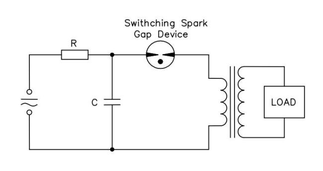
2RK-5 series Switching Spark Gaps(SSG) can be used in all applications where high voltage pulses are generated, for example to ignite modern high-pressure gas discharge lamps such as xenon lamps in automotive headlights. Ignition performance is determined to a large degree by the properties of the switching component. An extremely fast switch is called for, which operates virtually without loss and with high insulation resistance in the non-conducting state. It should also be as compact as possible, rugged, highly reliable, and capable of operating over a wide temperature range.

Features
Extremely long life time
Stable performance over life
Insensitive performance against variations in temperature
Low switching losses
Very short breakdown time
High reliability by robust design
Lead-free compliant
RoHS and REACH compliant
Non-Radioactive
Applications
Igniters for architectural and automotive Xenon discharge lamps
Electronic igniters for gas heating and gas domestic appliances, e.g., cookers
Ignition of ultra-high pressure gas discharge lamps for data and video projectors
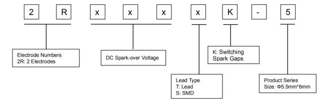
Part Number Code
Electrical Characteristics
| Part Number | DIP | 2R230TK-5 2R230SK-5 |
2R250TK-5 2R250SK-5 |
2R300TK-5 2R300SK-5 |
2R350TK-5 2R350SK-5 |
|||||||||||||||||||||||||||||||||||
| SMD | ||||||||||||||||||||||||||||||||||||||||
| Initial Values Static Breakdown Voltage VS @100V/S 1) First ignition Value after 24 hours in darkness Following Ignition Values |
<275 V 207~253 V | <300 V 225~275 V | <360 V 270~330 V | <420 V 315~385 V | ||||||||||||||||||||||||||||||||||||
| Electrical Life Time Breakdown Voltage VB 2) First ignition Value after 24 hours in darkness Following Ignition Values Switching Operations @ +25°C Breakdown Time Maximum Switching Frequency |
<285 V | <310 V | <370 V | <435 V | ||||||||||||||||||||||||||||||||||||
| 196~265 V 105 |
215~290 V 105 |
255~350 V 105 |
300~405 V 105 |
|||||||||||||||||||||||||||||||||||||
| <50 ns | <50 ns | <50 ns | <50 ns | |||||||||||||||||||||||||||||||||||||
| 100 Hz | 100 Hz | 200 Hz | 200 Hz | |||||||||||||||||||||||||||||||||||||
| Test Circuit Parameters | ||||||||||||||||||||||||||||||||||||||||
| Open Circuit Voltage V0 | 230 VAC | 350 V | 400 V | 450 V | ||||||||||||||||||||||||||||||||||||
| Loading Resistance R | 15 KΩ | 10 KΩ | 10 KΩ | 10 KΩ | ||||||||||||||||||||||||||||||||||||
| Discharge Capacitance C | 2.2 µF | 680 nF | 680 nF | 680 nF | ||||||||||||||||||||||||||||||||||||
| Inductance L | 10 µH | 0.5 µH | 0.5 µH | 0.5 µH | ||||||||||||||||||||||||||||||||||||
| Discharge Peak Current IP | ~300 A | ~500 A | ~500 A | ~500 A | ||||||||||||||||||||||||||||||||||||
| Part Number | DIP | 2R380TK-5 3) 2R380SK-5 3) |
2R400TK-5 2R400SK-5 |
2R450TK-5 2R450SK-5 |
2R470TK-5 2R470SK-5 |
|||||||||||||||||||||||||||||||||||
| SMD | ||||||||||||||||||||||||||||||||||||||||
| Initial Values Static Breakdown Voltage VS @100V/S 1) First ignition Value after 24 hours in darkness Following Ignition Values |
<460 V 350~420 V | <480 V 360~440 V | <540 V 405~495 V | <560 V 423~517 V | ||||||||||||||||||||||||||||||||||||
| Electrical Life Time Breakdown Voltage VB 2) First ignition Value after 24 hours in darkness Following Ignition Values Switching Operations @ +25°C Breakdown Time Maximum Switching Frequency |
<460 V | <500 V | <560 V | <585V | ||||||||||||||||||||||||||||||||||||
| 330~440 V 105 |
340~460 V 105 |
385~515 V 105 |
400~540 V 105 |
|||||||||||||||||||||||||||||||||||||
| <50 ns | <50 ns | <50 ns | <50 ns | |||||||||||||||||||||||||||||||||||||
| 200 Hz | 200 Hz | 200 Hz | 200 Hz | |||||||||||||||||||||||||||||||||||||
| Test Circuit Parameters | ||||||||||||||||||||||||||||||||||||||||
| Open Circuit Voltage V0 | 500 V | 520 V | 580 V | 600 V | ||||||||||||||||||||||||||||||||||||
| Loading Resistance R | 10 KΩ | 10 KΩ | 10 KΩ | 10 KΩ | ||||||||||||||||||||||||||||||||||||
| Discharge Capacitance C | 680 nF | 680 nF | 680 nF | 680 nF | ||||||||||||||||||||||||||||||||||||
| Inductance L | 0.5 µH | 0.5 µH | 0.5 µH | 0.5 µH | ||||||||||||||||||||||||||||||||||||
| Discharge Peak Current IP | ~500 A | ~500 A | ~500 A | ~500 A | ||||||||||||||||||||||||||||||||||||
| Part Number | DIP | 2R500TK-5 2R500SK-5 |
2R550TK-5 4) 2R550SK-5 4) |
2R600TK-5 2R600SK-5 |
||||||||||||||||||||||||||||||||||||
| SMD | ||||||||||||||||||||||||||||||||||||||||
| Initial Values Static Breakdown Voltage VS @100V/S 1) First ignition Value after 24 hours in darkness Following Ignition Values |
<600 V 450~550 V | <680 V 510~630 V | <720 V 540~660 V | |||||||||||||||||||||||||||||||||||||
| Electrical Life Time Breakdown Voltage VB 2) First ignition Value after 24 hours in darkness Following Ignition Values Switching Operations @ +25°C Breakdown Time Maximum Switching Frequency |
<625 V 425~575 V 105 <50 ns 200 Hz |
<710 V 485~655 V 105 <50 ns 200 Hz |
<750 V 510~690 V 105 <50 ns 200 Hz |
|||||||||||||||||||||||||||||||||||||
| Test Circuit Parameters Open Circuit Voltage V0 Loading Resistance R Discharge Capacitance C Inductance L Discharge Peak Current IP |
630 V 13 KΩ 470 nF 0.1 µH ~600 A |
720 V 13 KΩ 470 nF 0.1 µH ~600 A |
750 V 13 KΩ 470 nF 0.1 µH ~600 A |
|||||||||||||||||||||||||||||||||||||
| Insulation Resistance @100 V | >108 Ω | |||||||||||||||||||||||||||||||||||||||
| Capacitance @1MHz | <1 pF | |||||||||||||||||||||||||||||||||||||||
| Weight | DIP ~0.82g SMD ~0.55g | |||||||||||||||||||||||||||||||||||||||
| Operation and storage temperature | -40~+125°C | |||||||||||||||||||||||||||||||||||||||
| Surface treatment | DIP -Nickel Plated SMD -Matte-tin plated | |||||||||||||||||||||||||||||||||||||||
1) At delivery AQL 0.65 level II, DIN ISO 2859
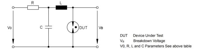
2) Fig. 1
3) 350 Marking
4) 600 Marking
Test Circuit Fig. 1
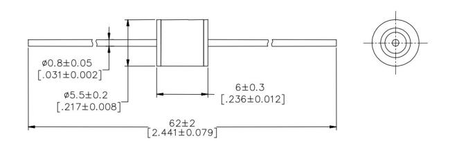
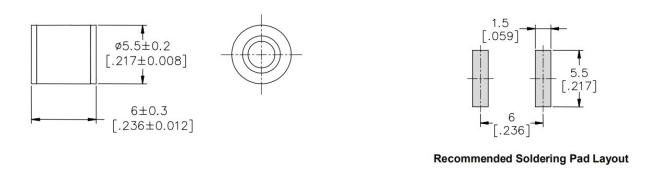
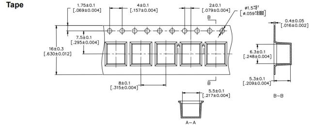
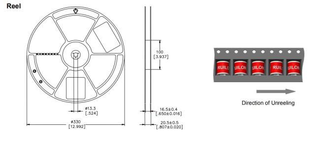
Dimensions (Unit: mm/inch)
DIP Series (2RxxxTK-5)
SMD Series (2RxxxSK-5)
Packaging Information (Unit: mm/inch)
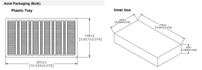
Packaging Quantity
100 PCS per Plastic Tray
5 Plastic Trays per inner box
500 PCS per inner box
Axial Packaging (Tape & Reel)
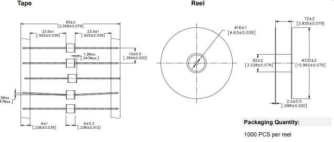
SMD Packaging (Tape & Reel)

Packaging Quantity
1,000 PCS per reel (13”)
3 reels per inner box
3,000 PCS per inner box
Basic Application Circuit
Soldering Parameters - Wave soldering (Thru-Hole Devices)
| Wave Soldering Condition | Pb-Free assembly | ||||||||||||||||||||
| Preheat | Temperature Min | 100°C | |||||||||||||||||||
| Temperature Max | 150°C | ||||||||||||||||||||
| Time (Min to Max) | 60-180 Seconds | ||||||||||||||||||||
| Solder Pot Temperature | 280°C Max | ||||||||||||||||||||
| Solder Dwell Time | 2-5 Seconds | ||||||||||||||||||||
Soldering Parameters - Reflow Soldering (Surface Mount Devices)
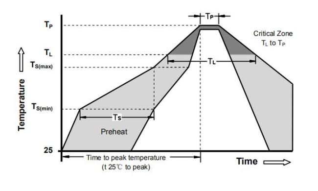
| Reflow Condition | Pb - Free assembly | ||||||||||||||||||||
| Preheat | -Temperature Min (Ts(min)) | 150°C | |||||||||||||||||||
| -Temperature Max (Ts(max)) | 200°C | ||||||||||||||||||||
| - Time (min to max) (ts) | 60 -180 Seconds | ||||||||||||||||||||
| Average ramp up rate ( Liquids Temp TL) to peak | 3°C/second max | ||||||||||||||||||||
| TS(max) to TL - Ramp-up Rate | 5°C/second max | ||||||||||||||||||||
| Reflow | - Temperature (TL) (Liquids) | 217°C | |||||||||||||||||||
| - Time (min to max) (ts) | 60 -150 Seconds | ||||||||||||||||||||
| Peak Temperature (TP) | 260 +0/-5°C | ||||||||||||||||||||
| Time within 5°C of actual peak Temperature (tp) | 10 - 30 Seconds | ||||||||||||||||||||
| Ramp-down Rate | 6°C/second max | ||||||||||||||||||||
| Time 25°C to peak Temperature (TP) | 8 minutes Max | ||||||||||||||||||||
| Do not exceed | 260°C | ||||||||||||||||||||
Similar Products
Get in Touch
Have questions about our products or want to discuss a custom order? Our team is ready to help you.
Company
Dongguan Tianrui Electronics Co., Ltd
Location
Building C, Xinmeijia Science and Technology Park, Chashan
Contact Person
Andy Wu