
IS61LPS25636A-200TQLI SRAM 8Mb 256Kx36 200Mhz Sync SRAM 3.3v Integrated Circuits ICs

IS61LPS25636A-200TQLI SRAM 8Mb 256Kx36 200Mhz Sync SRAM 3.3v
| ISSI | |
| Product Category: | SRAM |
| RoHS: | Details |
| 9 Mbit | |
| 256 k x 36 | |
| 3.1 ns | |
| 200 MHz | |
| Parallel | |
| 3.465 V | |
| 3.135 V | |
| 275 mA | |
| - 40 C | |
| + 85 C | |
| SMD/SMT | |
| TQFP-100 | |
| Tube | |
| Brand: | ISSI |
| Memory Type: | SDR |
| Moisture Sensitive: | Yes |
| Number of Ports: | 4 |
| Product Type: | SRAM |
| Series: | IS61LPS25636A |
| 72 | |
| Subcategory: | Memory & Data Storage |
| Type: | Synchronous |
| Unit Weight: | 0.023175 oz |
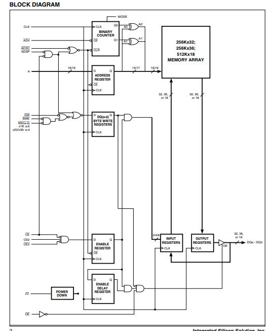
DESCRIPTION
The ISSI IS61LPS/VPS25636A, IS61LPS25632A,
IS64L PS25636A and IS61LPS/VPS51218A are high-
speed, low-power synchronous static RAMS designed
to provide burstable, high-performance memory for com-
munication and networking applications. The IS61LPS/
VPS25636A and IS64L PS25636A are organized as
262,144 words by 36 bits. The IS61LPS25632A is
organized as 262,144 words by 32 bits. The IS61LPS/
VPS51218A is organized as 524,288 words by 18 bits.
Fabricated with ISST's advanced CMOS technology,
the device integrates a 2-bit burst counter, high-speed
SRAM core, and high-drive capability outputs into asingle
monolithic circuit. All synchronous inputs pass through
registers controlled by a positive-edge-triggered single
clock input.
Write cycles are internally self-timed and are initiated by
the rising edge of the clock input. Write cycles can be
one to four bytes wide as controlled by the write control
inputs.
Separate byte enables allow individual bytes to be written.
The byte write operation is performed by using the byte
write enable (BWE) input combined with one or more
individual byte write signals (BWx). In addition, Global
Write (GW) is available for writing all bytes at one time,
regardless of the byte write controls.
Bursts can be initiated with either ADSP (Address Status
Processor) or ADSC (Address Status Cache Controller)
input pins. Subsequent burst addresses can be gener-
ated internally and controlled by the ADV (burst address
advance) input pin.
The mode pin is used to select the burst sequence or-
der, Linear burst is achieved when this pin is tied LOW.
Interleave burst is achieved when this pin is tied HIGH
or left floating.
FEATURES
●Internal self-timed write cycle
●Individual Byte Write Control and Global Write
●Clock controlled, registered address, data and
control
●Burst sequence control using MODE input
●Three chip enable option for simple depth ex-
pansion and address pipelining
●Common data inputs and data outputs
●Auto Power-down during deselect
●Single cycle deselect
●Snooze MODE for reduced-power standby
●JTAG Boundary Scan for BGA package
●Power Supply
LPS:VoD 3.3V 土5%, VoDa 3.3V/2.5V 土5%
VPS:VDD 2.5V土5%, VoDo 2.5V土5%
●JEDEC 100-Pin QFP, 119-ball BGA, and 165-
ball BGA packages
●Lead-free available


Get in Touch
Have questions about our products or want to discuss a custom order? Our team is ready to help you.