
TS5N214DBQR Digital Bus Switch ICs 2B 1of4 Fet Multipl/ Demult Hi-BW Bus Sw
Price:
Email us for details
MOQ:
1pcs
Delivery Time:
1day
Brand:
Texas Instruments
Product Description

TS5N214DBQR Digital Bus Switch ICs 2B 1of4 Fet Multipl/ Demult Hi-BW Bus Sw
| Texas Instruments | |
| Product Category: | Digital Bus Switch ICs |
| RoHS: | Details |
| 2 bit | |
| 3 Ohms | |
| 3 ns | |
| 5 V | |
| - 40 C | |
| + 85 C | |
| SMD/SMT | |
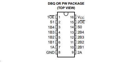
| SSOP-16 | |
| Reel | |
| Brand: | Texas Instruments |
| Moisture Sensitive: | Yes |
| Product Type: | Digital Bus Switch ICs |
| Series: | TS5N214 |
| Subcategory: | Switch ICs |
| Unit Weight: | 0.002628 oz |
Description
The TS5N214 is a high-bandwidth FET bus switch utilizing a charge pump to elevate the gate voltage of the pass
transistor, providing a low and flat ON-state resistance (ron). The low and flat ON-state resistance allows for
minimal propagation delay and supports rail-to-rail switching on the data input/output (I/O) ports. The device also
features low data /O capacitance to minimize capacitive loading and signal distorion on the data bus. Specifically
designed to support high-bandwidth applications, the TS5N2 14 provides an optimized interface solution ideally
suited for broadband communications, networking, and data-intensive computing systems.
The TS5N214 is a 2-bit 1-of-4 multiplexer/demultiplexer with separate output-enable (1OE, 20E) inputs. The
select (S0, S1) inputs control the data path of the multiplexer/demultiplexer. When OE is low, the
multiplexer/demultiplexer is enabled and the A port is connected to the B port, allowing bidirectional data flow
between ports. When OE is high, the multiplexer/demultiplexer is disabled and a high-impedance state exists
between the A and B ports.
This device is fully specified for partial-power-down applications using lff The lof circuitry prevents damaging
current backflow through the device when it is powered down. The device has isolation during power off.
To ensure the high-impedance state during power up or power down, OE should be tied to Voc through a pullup
resistor; the minimum value of the resistor is determined by the current-sinking capability of the driver.
FEATURES
• Low and Flat ON-State Resistance (ron)Characteristics Over Operating Range(ron = 3 Ω Typ)
• 0- to 10-V Switching on Data I/O Ports• Bidirectional Data Flow With Near-ZeroPropagation Delay
• Low Input/Output Capacitance MinimizesLoading and Signal Distortion(Cio(OFF) = 20 pF Max, B Port)
• VCC Operating Range From 4.75 V to 5.25 V
• Latch-Up Performance Exceeds 100 mA PerJESD 78, Class II
• ESD Performance Tested Per JESD 22– 2000-V Human-Body Model(A114-B, Class II)– 1000-V
Charged-Device Model (C101)
• Supports Both Digital and AnalogApplications: PCI Interface, Differential SignalInterface, Memory Interleaving,
Bus Isolation,Low-Distortion Signal Gating


Similar Products
Get in Touch
Have questions about our products or want to discuss a custom order? Our team is ready to help you.
Company
Wisdtech Technology Co.,Limited
Location
Room 1205-1207, Nanguang building, Huafu Road, Futian District, Shenzhen, Guangdong, China
Contact Person
Tao