
Tailored Copper Thick Green Solder Multi Layer PCB Board Higher Reliability
10 layer FR4 Green Solder Multi-layer PCB Board PCB
FR4 Multilayer PCB board is a printed circuit board composed of three or more layers of circuits. Each layer of circuits is composed of different circuit layers, and these layers are connected together through vias or interconnecting lines. Compared with single-sided and double-sided PCBs, multi-layer PCBs can achieve more circuit wiring in a smaller space and are suitable for more complex and function-intensive circuit designs.
Advantages of Multilayer PCB:
1.Structural Feature: Multiple copper circuit layers separated by insulating prepreg, bonded into an integrated rigid/flexible board via high-temperature lamination.
2.Interconnection Method: Uses through, blind, or buried vias to realize electrical connection between internal and external circuit layers.
3.Performance Trait: Excellent impedance control, low signal crosstalk, strong anti-interference ability, suitable for high-frequency and high-speed signal transmission.
4.Design Advantage: High-density wiring in a small footprint, supports complex multi-functional circuit layouts and product miniaturization.
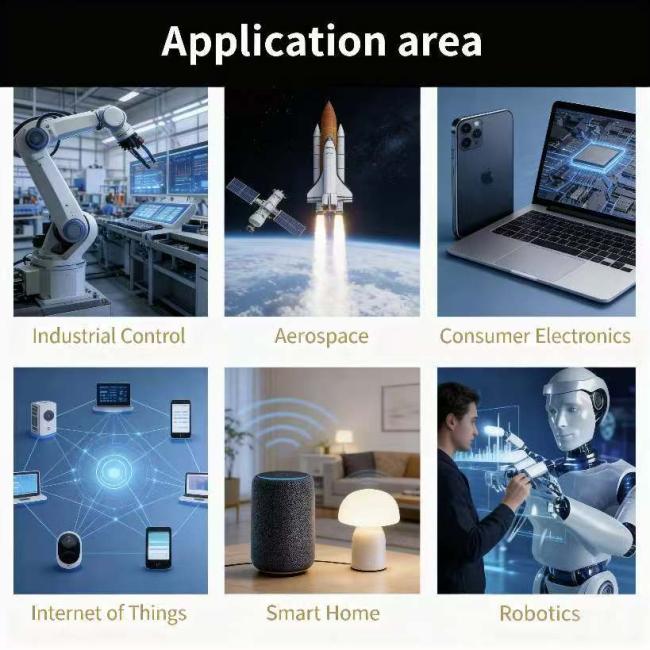
5.Application Adaptability: Compatible with harsh working environments; widely used in high-end electronics like 5G equipment, automotive electronics and aerospace devices.
Why choose our multilayer printed circuit boards?
✔ 30 Years Expertise in PCB Manufacturing
✔ ISO 9001, ROHS, and ISO /TS16949 Certified
✔ Support customized services
✔ Professional Engineering Support (DFM, impedance simulation)
✔ Global Shipping (DHL, FedEx, UPS) – Delivered to USA, Germany, UK, Japan, Australia, etc.
Manufacturing Process of Multilayer PCBs
1. Inner-layer Core Fabrication: Transfer circuit patterns onto copper-clad laminates, etch excess copper, and strip photoresist to form inner circuits.
2. AOI Inspection: Check inner boards for defects like open/short circuits with automated optical inspection.
3. Layer Stacking & Lamination: Alternate inner cores with prepreg, then press under high temperature and pressure to bond into an integrated block.
4. Drilling: Drill through, blind or buried vias at designated positions for interlayer connections.
5. Plating: Plate copper on via walls and board surfaces to ensure electrical conductivity between layers.
6. Outer-layer Processing: Repeat pattern transfer and etching to create outer circuit traces.
7. Surface Finishing: Apply HASL, ENIG or immersion tin to protect copper and improve solderability.
8. Final Testing & Shaping: Conduct electrical tests, trim to size, and perform quality checks before packaging.

Factory showcase

PCB Quality Testing

Certificates and Honors

Get in Touch
Have questions about our products or want to discuss a custom order? Our team is ready to help you.