
OEM High Density PCB Manufacturing ENIG Surface Finish&Blind Buried Vias Design
What is an HD circuit board?:
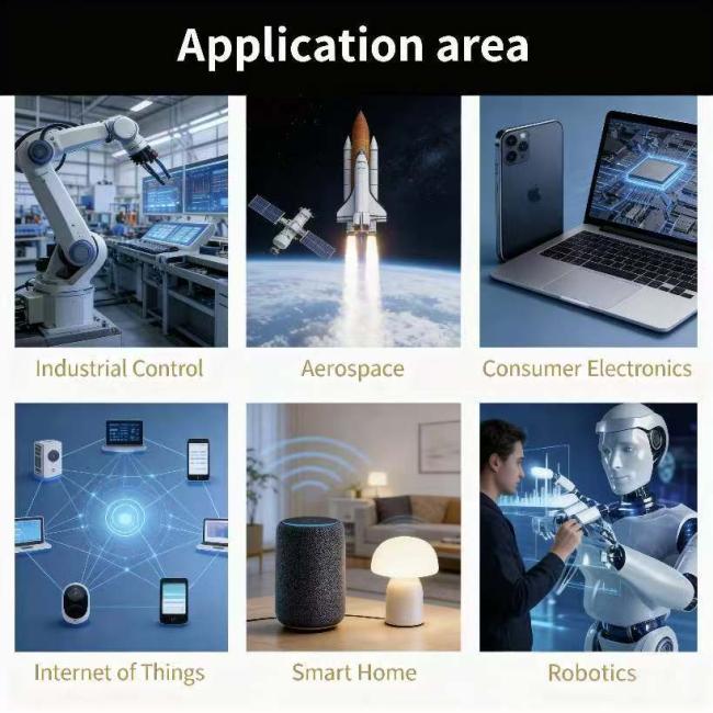
HD PCB (High Density PCB) is an advanced type of printed circuit board designed for high component density, miniaturization, and high-performance electronic devices.Compared to traditional PCBs, it features ultra-fine copper traces (line widths/spacings usually ≤ 0.1mm, even down to 0.03mm), tiny microvias (diameter ≤ 0.15mm, in blind/buried/stacked designs), and more layers (often 8–40+ layers). It also uses specialized materials (e.g., high-heat-resistant high-Tg FR-4, flexible polyimide) and strict manufacturing precision to support dense component mounting (e.g., fine-pitch chips).Widely used in smartphones, wearables, EVs, medical implants, and 5G equipment, it enables smaller device sizes, stable high-speed signal transmission, and reliable operation in harsh environments.
Custom HDI PCB – Signal Optimized & Cost Effective :
1. Enables device miniaturization: Ultra-fine traces, microvias, and multi-layer designs let more components fit in small spaces, supporting slim/portable devices (e.g., smartwatches, thin smartphones).
2. Boosts signal performance: Low-loss materials and short microvia paths reduce signal interference and weakening, critical for high-speed/high-frequency devices (e.g., 5G modems, LiDAR).
3. Enhances reliability: Fewer connectors (replacing multiple traditional PCBs) and harsh-environment-resistant substrates (e.g., high-Tg FR-4) lower failure risks, suitable for autos/aerospace.
4. Frees up design flexibility: Supports flexible structures (foldable phones) and stacked components (e.g., memory on CPU), easing integration of complex functions.
5. Cuts long-term costs: Though upfront manufacturing is pricier, smaller device size, fewer assembly steps, and less maintenance reduce overall expenses.
How is the manufacturing process of HDPCB?
1. DFM & Custom Confirmation:Finalize Gerber files, layer count, materials, surface finish and customer specs; complete DFM check.
2. Inner Layer Processing:Etch inner circuits, conduct AOI inspection.
3.Lamination:Stack and press inner layers with prepregs into a multilayer core.
4.Laser Drilling & Plating:Drill microvias/through holes; metallize vias for conduction.
5.Outer Layer & Surface Treatment:Etch outer circuits, apply solder mask and chosen surface finish.
6.Silkscreen & Profiling:Print markings; rout to final board shape.
7.Electrical Test & QA:Perform open/short and impedance testing; verify quality standards.
8.Packaging & Delivery:Anti-static vacuum packaging and shipment.

Factory showcase

PCB Quality Testing

Certificates and Honors

Get in Touch
Have questions about our products or want to discuss a custom order? Our team is ready to help you.