
Premium Green Oil Multi-Layer HDI Circuit Board with ENIG Surface and High TG Material
Why choose Multi-Layer HDI Circuit Board ?:
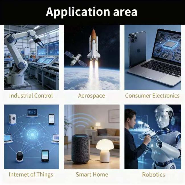
Built with high-quality materials and strict manufacturing standards, this multi-layer PCB delivers exceptional stability and durability. The ENIG coating provides excellent protection against oxidation and corrosion, ensuring long-term performance even in harsh environments. With its reliable power distribution and enhanced signal integrity, this board is perfectly suited for automotive electronics, medical equipment, and IoT devices that require consistent operation and resistance to temperature fluctuations.
The advantages of Multi-Layer HDI PCBs :
| Feature / Feature | Multi-Layer HDI PCB (Your Product) | Standard Multi-Layer PCB | Single/Double Layer PCB |
|---|---|---|---|
| Size & Weight | Ultra-Compact (30-50% smaller) | Standard Size | Bulky / Large |
| Component Density | High (Supports tiny BGA/QFN) | Medium | Low (Limited to through-hole) |
| Signal Performance | Excellent (Short paths, low noise) | Good | Poor (Long traces, crosstalk) |
| Reliability | High (Fewer via failures) | Medium | Medium |
| Design Flexibility | Very High (Blind/Buried Vias) | Limited (Mainly Through-Holes) | Very Limited |
| Ideal For | 5G, Phones, IoT, High-Speed Data | Industrial Control, Power | Simple Toys, Basic Circuits |
Custom Production Process for Multi-Layer HDI PCBs:
1.Design Review
First, our engineers check your Gerber files and design data to ensure they meet HDI manufacturing requirements, including trace widths, via sizes, and layer stack‑up.
2.Layer Stack‑up & Material Selection
We select the appropriate materials, such as FR‑4 or high‑TG laminates, and create the multi‑layer stack‑up with signal, power, and ground planes.
3.Laser Drilling for HDI Vias
For HDI boards, we use laser drilling to create small blind and buried vias, which allow connections between inner layers without going through the entire board.
4.Plating & Copper Deposition
The vias are plated with copper to make them electrically conductive, ensuring reliable connections between layers.
5.Lamination
Multiple layers are bonded together under high temperature and pressure to form a solid, unified multi‑layer board.
6.Outer‑Layer Imaging & Etching
The outer‑layer circuits are imaged, etched, and cleaned to create the final trace patterns.
7.Surface Finish (ENIG)
An ENIG finish is applied to provide excellent solderability, corrosion resistance, and long‑term reliability.
8.Electrical Testing
The board undergoes rigorous electrical testing to ensure there are no shorts, opens, or impedance issues.
9.Quality Inspection & Packing
Finally, the PCBs are inspected for quality, then packed and prepared for shipment.

Factory showcase

PCB Quality Testing

Certificates and Honors

Get in Touch
Have questions about our products or want to discuss a custom order? Our team is ready to help you.