
Sub-1% Capacitance Matched MOS Capacitor 220pF 100V CTE Optimized Single Layer Chip For GaN SiC Power Modules
HACC221S100V502 Precision MOS Capacitor — 220 pF 100 V with Sub-1% Capacitance Matching and CTE Optimization for GaN & SiC Power Substrates
The HACC221S100V502 is a 220 pF ±10% single-layer MOS (metal-oxide-semiconductor) capacitor rated at 100 V DC, fabricated on float-zone silicon (>1000 Ω·cm) with 300 nm-class thermal SiO2 dielectric and TiW-Au / TiW-Pt-Au metallization. Standard chip outline is 0.55 mm × 0.55 mm × 0.18 mm (±25 µm). It is engineered for wide-bandgap power modules where pair-to-pair capacitance symmetry and thermo-mechanical reliability under power cycling determine circuit performance.
Because the silicon MOS structure is formed directly on a single-crystal silicon substrate, its coefficient of thermal expansion (CTE, 2.6 ppm/°C) is inherently close to that of silicon-carbide and GaN-on-SiC power devices — an advantage over alumina-based ceramic capacitors when co-packaged on power substrates.
Sub-1% Precision Capacitance Matching across Wafers
- Wafer-level sorting service: capacitors are 100% electrically probed and sorted so that matched sets shipped together stay within <1% capacitance spread, across wafer position, wafer-to-wafer and lot-to-lot;
- Matched pairs and arrays are shipped with digital wafer map documentation and full lot traceability per wafer lot;
- Ultra-stable thermal SiO2 dielectric keeps matching drift small over the full -55°C to +200°C range and under DC bias (TCC +35 ppm/°C);
- Ideal for balanced half-bridge gate drive, snubber and divider networks where capacitance symmetry controls switching balance and EMI.
Electrical Characteristics (typical, 25°C unless noted)
| Nominal Capacitance | 220 pF ±10% (1 kHz, 1.0 Vrms); matched sets with <1% spread available |
| Rated Voltage | 100 V DC |
| Dielectric Withstanding Voltage | 250 V DC (250% rated, 5 s, 100% tested) |
| Temperature Coefficient (TCC) | +35 ppm/°C over -55°C to +200°C |
| Dissipation Factor | ≤0.15% at 1 kHz, 1.0 Vrms |
| Q Factor | >2000 at 1 MHz; >200 at 1 GHz |
| ESR at 1 GHz | <0.1 Ω |
| Intrinsic Chip ESL | <0.05 nH (de-embedded); chip-level SRF >1.5 GHz; system SRF >500 MHz with 0.5 mm Au bond wire |
| Leakage Current | <10 nA at 25°C; <500 nA at 200°C (at rated voltage) |
| Insulation Resistance | ≥104 MΩ at rated voltage, 25°C |
| ESD Tolerance | >2 kV HBM, Class 2 per JESD22-A114 |
| Operating / Storage Temperature | -55°C to +200°C / -65°C to +150°C |
| Standard Die Size | 0.55 × 0.55 × 0.18 mm (±25 µm); custom geometry, aspect ratio up to 4:1 |
| Metallization | TiW-Au top (≥2.5 µm Au, wire bondable); TiW-Pt-Au backside (AuSn / solder / silver epoxy) or Au-only backside |
Typical Applications
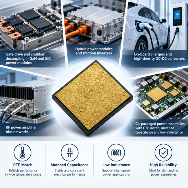
Gate drive and snubber decoupling in GaN and SiC power modules; hybrid power modules and traction inverters; on-board chargers and high-density DC-DC converters; RF power amplifier bias networks; and any co-packaged power assembly where CTE match, matched capacitance and low inductance are required.
Get in Touch
Have questions about our products or want to discuss a custom order? Our team is ready to help you.