
Nanoscale Staggered Guard-Ring MOS Capacitor 1000pF 50V Single Layer Chip For Pico-Amp Leakage
HACC102S50V300 Nanoscale Staggered Guard-Ring MOS Capacitor — 1000pF 50V Single Layer Chip
Product overview: The HACC102S50V300 is a single-layer metal-oxide-semiconductor (MOS) capacitor with a nominal capacitance of 1000pF (1nF) ±10% and a 50V DC working voltage. It uses a 300nm thermal silicon dioxide (SiO2) dielectric on a float-zone silicon substrate with a TiW-Au metallization stack. Its defining feature is a nanoscale staggered guard-ring around the top electrode, which lengthens the surface leakage path and confines the electric field so that leakage current stays in the pico-amp range. It suits precision and high-impedance RF and analog circuits where leakage directly limits accuracy.
What Is a Nanoscale Staggered Guard-Ring?
A guard ring is a conductive or insulating structure placed around the active electrode to intercept surface leakage current and keep it away from the signal path. A staggered guard-ring uses several closely spaced nanoscale rings rather than a single large one. This increases the effective surface path length and spreads the electric field across multiple steps, so the field at any single point is lower and the surface leakage that would otherwise flow between terminals is strongly reduced. The result is leakage in the pico-amp range, which matters in high-impedance circuits where even nanoamp leakage would load or offset the signal.
Guard-Ring Design Notes
- Field spreading: each step in the staggered ring reduces the peak electric field, and the field is distributed over more surface area.
- Longer surface path: multiple closely spaced rings increase the distance leakage current must travel along the surface.
- High-resistivity substrate: float-zone silicon above 1000 Ω·cm limits bulk leakage between the top electrode and the substrate.
- Dense thermal oxide: the dielectric has low defect density, so bulk leakage through the oxide stays low across temperature.
Key Specifications (T = 25°C unless noted)
| Parameter | Value | Condition |
| Capacitance | 1000pF (1nF) ±10% | 1MHz, 1.0Vrms |
| Rated DC voltage | 50V | Continuous |
| Dielectric strength | >125V DC | 1 minute, 25°C |
| Leakage current | <100 pA | 50V DC, 25°C, typical |
| Guard-ring design | Nanoscale staggered multi-ring | Surface leakage suppression |
| Intrinsic chip ESL | <0.05nH | De-embedded from S-parameters |
| Q factor at 1MHz | >2000 | Typical |
| Dielectric absorption | <0.1% | Typical |
| TCC | +35ppm/°C | -55°C to +125°C |
| Dielectric | Thermal SiO2, 300nm | Low defect density |
| Substrate | Float-zone Si, >1000 Ω·cm | High-resistivity |
| Chip dimensions | 0.50 × 0.50 × 0.15mm | ±0.025mm |
| Top metallization | TiW + Au, 2.5µm min | Wire bondable |
| Backside metallization | TiW-Pt-Au, Au 1.0µm min | Die attach |
| Operating temperature | -55°C to +125°C | — |
| RoHS | Compliant | EU 2015/863 |
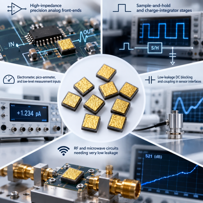
Typical Applications
- High-impedance precision analog front-ends
- Sample-and-hold and charge-integrator stages
- Electrometer, pico-ammeter, and low-level measurement inputs
- Low-leakage DC blocking and coupling in sensor interfaces
- RF and microwave circuits needing very low leakage
Get in Touch
Have questions about our products or want to discuss a custom order? Our team is ready to help you.