
Zero Defect BGA Assembly X Ray Certified PCB Board Manufacturer

Overview
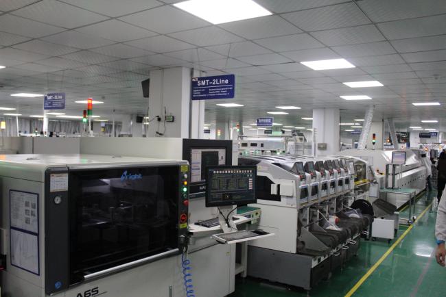
Zero-defect quality is the standard for critical BGA applications—medical devices, automotive safety systems, aerospace electronics. Studio Electronics offers Zero-Defect BGA Assembly with X-Ray certified quality—ensuring every BGA on every board meets the most stringent quality requirements. As a premier provider of PCB assembly in China, we combine specialized BGA process expertise, 12 automated SMT lines, advanced 3D X-Ray inspection, and rigorous process control to deliver assemblies with documented, verifiable quality. Our complete turnkey service covers component procurement through final shipping.

| Quality Element | Studio's Capability | Verification Method |
|---|---|---|
| Process Control | Optimized reflow profiles; nitrogen reflow; controlled parameters | Real-time monitoring; documented profiles |
| 100% X-Ray Inspection | 2D and 3D X-Ray on every BGA board | Automated void analysis; ball position verification |
| Void Control | <10% void target for critical applications | 3D X-Ray; void data per ball serial number |
| Electrical Testing | ICT; Flying Probe; FCT—100% coverage | Documented test results per board |
| Traceability | MES records; component lot tracking; X-Ray images | Complete documentation per board serial number |
| Documentation | X-Ray images; test reports; process records | Audit-ready quality package |


Stage 1: Component Sourcing
Components sourced through authorized distributors. For low volume PCB assembly, small-quantity procurement supported. Incoming inspection verifies component integrity and BGA ball condition.
Stage 2: Solder Paste Printing
Precision stencil with optimized aperture geometry. 3D SPI ensures consistent paste deposition; real-time feedback corrects printing variations.
Stage 3: Precision BGA Placement
12 SMT lines with ±25μm accuracy. Vision alignment ensures accurate ball-to-pad registration. Placement parameters optimized per BGA type.
Stage 4: Controlled Reflow
Custom reflow profiles per BGA type. Nitrogen reflow minimizes voiding. Closed-loop temperature control; real-time monitoring.
Stage 5: 100% X-Ray Certification
-
2D X-Ray – Ball alignment, bridging, missing balls
-
3D X-Ray – Void analysis; automated void calculation
-
Void Target – <10% for critical applications; <15% for standard
-
Certification – X-Ray verified; documented per board serial number
Stage 6: Testing & Final Assembly
ICT; Flying Probe; FCT; AOI for visible components. Reliability lab testing available. Careful handling; anti-static packaging; global logistics.


| Quality Requirement | Studio's Zero-Defect Solution |
|---|---|
| Hidden defects | 3D X-Ray detects all voiding; bridging; cold joints |
| Process variation | Controlled reflow; real-time monitoring |
| Documentation | Complete quality records per board serial number |
| Regulatory compliance | Documented inspection supports FDA/ISO submissions |
| Field reliability | Zero-defect quality ensures reliable product performance |
Studio delivers Zero-Defect BGA Assembly—X-Ray certified quality with complete documentation per board serial number.
Get in Touch
Have questions about our products or want to discuss a custom order? Our team is ready to help you.