
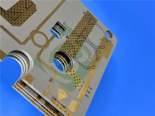
RF-10 high frequency material PCB 2-Layer Copper Clad Laminate 10mil Core with ENIG Finish using in Microstrip Patch Antennas
RF-10 PCB: 2-Layer, 10mil Core, Immersion Gold Finish
(All PCBs are custom-manufactured. Reference images and parameters may vary based on your design requirements.)
Overview of the 2-Layer RF-10 PCB
The 2-layer RF-10 PCB is a high-performance, ceramic-filled PTFE laminate designed for RF and microwave applications requiring high dielectric constant (Dk), low insertion loss, and outstanding dimensional stability. With its 10mil (0.254mm) core, immersion gold (ENIG) surface finish, and precise construction, this PCB supports miniaturized designs for high-frequency applications like microstrip patch antennas, GPS systems, and satellite components.
PCB Construction Details
| Parameter | Specification |
| Base Material | RF-10 |
| Layer Count | 2 layers |
| Board Dimensions | 45mm x 50mm ± 0.15mm |
| Minimum Trace/Space | 6/5 mils |
| Minimum Hole Size | 0.3mm |
| Blind Vias | No |
| Finished Board Thickness | 0.3mm |
| Copper Weight | 1oz (1.4 mils) outer layers |
| Via Plating Thickness | 20 μm |
| Surface Finish | Immersion Gold (ENIG) |
| Top Silkscreen | None |
| Bottom Silkscreen | None |
| Top Solder Mask | None |
| Bottom Solder Mask | None |
| Electrical Testing | 100% tested prior to shipment |
PCB Stackup
| Layer | Material | Thickness |
| Copper Layer 1 | Copper (1oz) | 35 μm |
| Core Material | RF-10 Ceramic PTFE | 10mil (0.254mm) |
| Copper Layer 2 | Copper (1oz) | 35 μm |
PCB Statistics
The compact 2-layer RF-10 PCB is designed for simplified but reliable layouts. Below are the key statistics:
- Components: 7
- Total Pads: 29
- Thru Hole Pads: 21
- Top SMT Pads: 8
- Bottom SMT Pads: 0
- Vias: 14
- Nets: 2
Introduction to RF-10 Material
RF-10 laminates are composites of ceramic-filled PTFE reinforced with woven fiberglass. These materials are engineered to deliver high dielectric constant, low dissipation factor, and excellent dimensional stability.
Key attributes include:
- High thermal conductivity: Efficient heat dissipation for thermal management.
- Low dissipation factor: Minimizes signal loss at high frequencies.
- Tight Dk tolerance: Ensures consistent performance across applications.
Features of RF-10
- Dielectric Constant (Dk): 10.2 ± 0.3 at 10GHz
- Dissipation Factor (Df): 0.0025 at 10GHz
- Thermal Conductivity: 0.85 W/mK (unclad)
- Coefficient of Thermal Expansion (CTE): X-axis: 16 ppm/°C, Y-axis: 20 ppm/°C, Z-axis: 25 ppm/°C
- Moisture Absorption: 0.08%
- Flammability Rating: UL-94 V0
Benefits of RF-10 PCB
- High Dielectric Constant (Dk): Enables size reduction for RF circuits.
- Low Dissipation Factor: Minimizes phase shift and insertion loss.
- High Thermal Conductivity: Improves heat dissipation for better performance.
- Excellent Dimensional Stability: Ensures high production yields and reliability.
- Smooth Copper Bonding: Reduces skin-effect losses at high frequencies.
- Low Moisture Absorption: Maintains performance in humid environments.
- Cost-Effective: Delivers excellent performance at a competitive price.
Applications of RF-10 PCB
- Microstrip Patch Antennas
- GPS Antennas
- Passive Components:
- Aircraft Collision Avoidance Systems
- Satellite Components
Why Choose the 2-Layer RF-10 PCB?
The 2-layer RF-10 PCB is a reliable solution for high-frequency circuit designs requiring low loss, compact size, and thermal stability. Its 10mil core, ENIG finish, and high Dk make it an ideal choice for aerospace, telecommunications, and satellite systems.
Contact us today to learn more about this high-performance PCB or to place your order!
Get in Touch
Have questions about our products or want to discuss a custom order? Our team is ready to help you.