
3inch 4inch 6Inch 900 Nm LT LN thin film Y-42° commen
3inch 4inch 6Inch 900 Nm LT LN thin film Y-42° commen
Lithium Tantalate exhibits unique electro-optical, pyroelectric and piezoelectric properties combined with good mechanical and chemical stability and , wide transparency range and high optical damage threshold.
Characterisation of LTThin Films
Thin LiTaO3 films were prepared by spin coating of polymerized sol-gel precursor solution. Films have been deposited on single crystal silicon substrate, Ti/Pt or SiO2 coated silicon substrate. Films were characterized by x-ray diffraction, dielectric and pyroelectric Measurements. High Curie temperature (above 550 °C) was assumed for LiTaO3 thin films from the temperature dependence of dielectric constant. Replacing 35% of tantalum by titanium atoms in the LiTaO3 precursor solution has resulted the thin films with Curie temperature of 330 °C. The lower Curie temperature leads to the larger pyroelectric coefficient at room-temperature, which is more than double that of the undoped LiTaO3 thin films. The dielectric, pyroelectric, and ferroelectric properties have been compared to the single crystal LiTaO3 and ceramic Li0.91Ta0.73Ti0.36O3. LiTaO3 thin films are available by sol-gel process at low temperature, and their properties may possibly be controlled by varying the composition of the sol-gel precursor solution.
Piezoelectric Crystal LiTaO3 thin film/wafer
| Specification | Conventional | High Precision |
| Materials | LiTaO3(LT)/ LiNbO3 wafers | LiTaO3(LT)/LiNbO3 wafers |
| Orientation | X-112°Y,36°Y,42°Y±0.5° | X-112°Y,36°Y,42°Y±0.5° |
| Parallel | 30″ | 10'' |
| Perpendicular | 10′ | 5' |
| surface Quality | 40/20 | 20/10 |
| Wavefront Distortion |
λ/4@632nm |
λ/8@632nm |
| Surface Flatness |
λ/4@632nm |
λ/8@632nm |
| Clear Aperture | >90% | >90% |
| Chamfer | <0.2×45° | <0.2×45° |
| Thickness/Diameter Tolerance | ±0.1 mm | ±0.1 mm |
| Maximum dimensions | dia150×50mm | dia150×50mm |
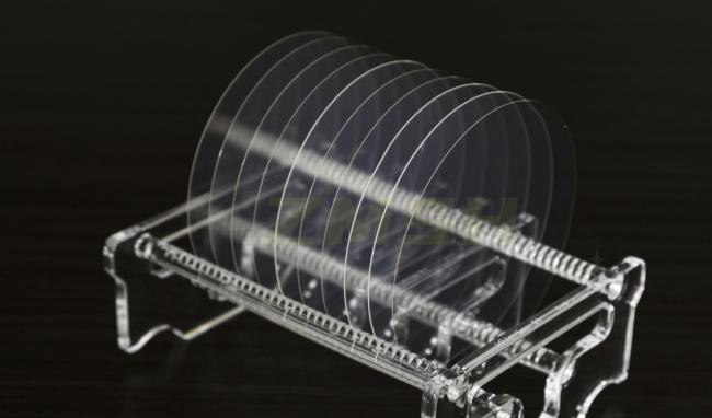
Product display

FAQ
Q. Do you have any stock of wafer or ingots?
yes,aslike 3inch,4inch commen size substrates wafers are in stocks.
Q. Where is your company located?
Our company located in shanghai,China. factory is in wuxi city.
Q. How long will take to get the products?
Generally it will take 1~4 weeks to process and then delivery.
It is depend on the quantity and the size of the products.
Q: How about pay term & delivery ?
T/T 50%deposit and left part before delivery by FOB .
Get in Touch
Have questions about our products or want to discuss a custom order? Our team is ready to help you.