
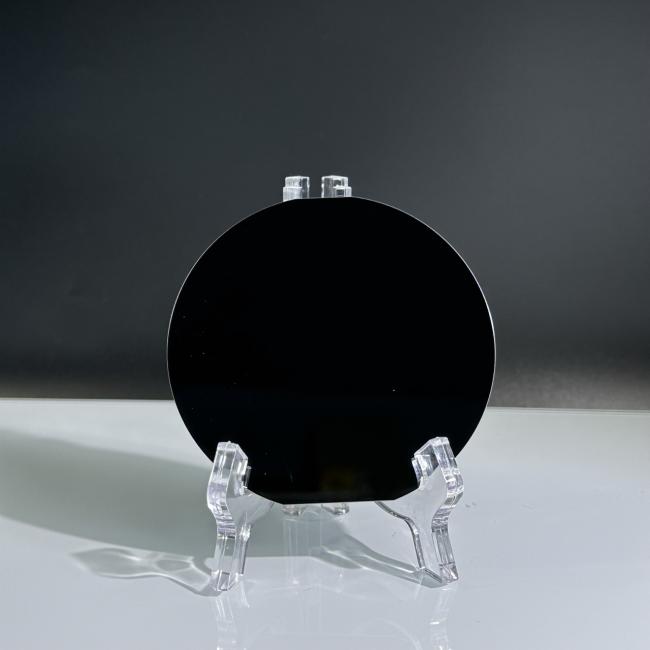
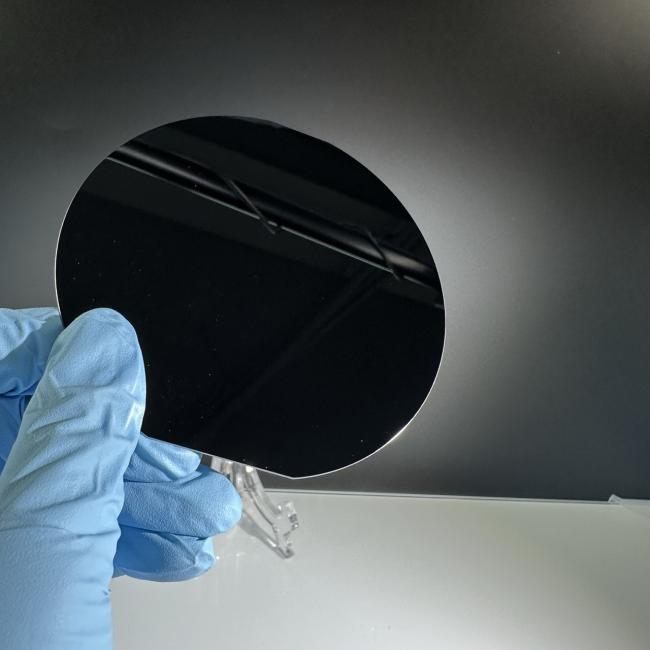
4'' 6'' AIN On Silicon Substrates SSP DSP Semiconductor Wafers 100nm 200nm Layer
4'' 6'' AIN On Silicon Substrates SSP DSP Semiconductor Wafers 100nm 200nm Layer
Description:
Aluminum Nitride on Silicon Wafers is a new type of semiconductor material that offers unique properties. The aluminum nitride ceramic has a low dielectric constant and excellent mechanical properties. It is non-toxic and has a linear expansion coefficient similar to that of silicon. In addition, it has low thermal conductivity. This combination of properties makes aluminum nitride an ideal material for many electronic applications. A thin film of aluminum nitride is a form of semiconductor material. It is highly conductivealuminum nitride on silicon wafers and can withstand high temperatures. It is also resistant to electromagnets and has a high boiling point. As a result, it is commonly used in mobile phones and other electronics. However, it is not advisable to process Aluminum Nitride on Silicon Wafers without proper annealing.
Specification:
- Useful area: 90%
-
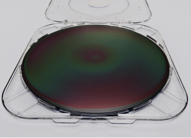
Nominal AlN thickness: 200nm ± 5%, one side coated, undoped AlN film
-
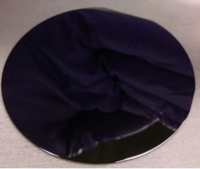
Front Surface: As-grown
-
Back surface: Silicon as received
-
AlN orientation: C-plane (001)
-
Macro Defect Density: <5/cm^2
-
Wafer base: Silicon [111] N type, 2" dia x0.5 mm, Resistivity: <5 ohm-cm, one side polished
Application:
- Aluminum nitride on silicon wafers is an ideal substrate material for many applications. It has similar thermal expansion properties to silicon wafers and is chemically inert. Its high thermal conductivity and low resistance make it a suitable material for many electronic applications. This makes aluminum nitride on silicon the best choice for electronics. And it's environmentally friendly.
- Compared with silicon, aluminum nitride on silicon has excellent electrical conductivity and lower coefficient of thermal expansion. These properties make it an excellent semiconductor material. In addition to electronics, it is also safe for the environment.
- Aluminum nitride on silicon wafers is an excellent alternative to beryllium oxide in electronics applications. Its low cost and non-toxic properties make it an ideal alternative to silicon wafers. This semiconductor material can also be used in electronic applications.
- The material is extremely durable. It is suitable for a variety of electronic applications. Its low thermal conductivity and high electrical insulation make it an excellent material for electronic devices. Unlike silicon, it is non-toxic and easy to make. In addition to electronic applications, it also has a low dielectric constant. It is also an excellent substitute for silicon in high-speed lasers.
Other Product:
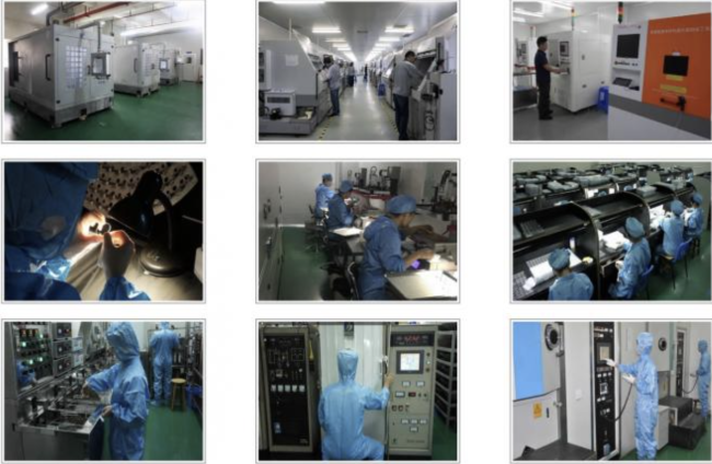
Company Introduction:
Get in Touch
Have questions about our products or want to discuss a custom order? Our team is ready to help you.