
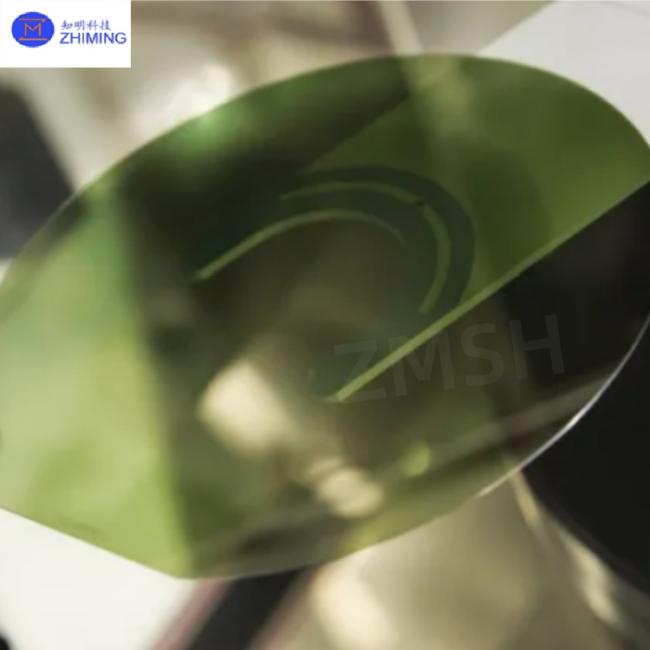
SiC Crystal Seed Wafers Dia 205 203 208 Production Grade PVT/HTCVD Growth
Abstract of SiC seed wafer
SiC crystal seed wafers Dia 205 203 208 Production Grade PVT/HTCVD growth
Silicon Carbide (SiC) Seed Crystal Wafers are the foundational materials for SiC single-crystal growth and device fabrication, produced through cutting, grinding, and polishing of high-purity SiC crystals. These wafers exhibit ultra-high thermal conductivity (4.9 W/cm·K), exceptional breakdown field strength (2–4 MV/cm), wide bandgap (3.2 eV), and chemical inertness, making them critical for applications in extreme environments such as aerospace, nuclear energy, and high-power electronics. Serving as the "seed" for crystal growth, their crystallographic orientation (e.g., 4H-SiC polytype), surface flatness, and micropipe density directly influence the quality of downstream ingots and device performance. ZMSH provides 2–12-inch SiC seed crystal wafers with diameters of 153mm, 155mm, 203mm, 205mm, and 208mm, catering to semiconductor, renewable energy, and industrial sectors.
Key Features of SiC seed wafer

1. Physical and Chemical Superiority
- Extreme Durability: SiC Seed Crystal Wafers withstand temperatures exceeding 1700°C and radiation exposure, ideal for aerospace and nuclear applications.
- Electrical Performance: High electron saturation velocity (2.7×10⁷ cm/s) enables high-frequency devices (e.g., 5G RF amplifiers).
- Defect Control: Micropipe density <1 cm⁻² and minimal polytype defects ensure uniform ingot growth.
2. Advanced Fabrication Processes
- Crystal Growth: SiC Seed Crystal Wafers utilizes Physical Vapor Transport (PVT) or High-Temperature Chemical Vapor Deposition (HTCVD) to precisely control temperature gradients and precursor transport.
- Processing Techniques: SiC Seed Crystal Wafers employs multi-wire sawing, diamond grinding, and laser stealth dicing to achieve surface roughness ≤Rz0.1μm and ±0.1mm dimensional accuracy.
3. Flexible Specifications
- Size Diversity: SiC Seed Crystal Wafers support 2–12-inch wafers (153–208mm diameter), adaptable to power devices, RF modules, and sensor applications.
Technical specifications of SiC seed wafers
|
Silicon carbide seed wafer |
|
|
Polytype |
4H |
|
Surface orientation error |
4°toward<11-20>±0.5º |
|
Resistivity |
customization |
|
Diameter |
205±0.5mm |
|
Thickness |
600±50μm |
|
Roughness |
CMP,Ra≤0.2nm |
|
Micropipe Density |
≤1 ea/cm2 |
|
Scratches |
≤5,Total Length≤2*Diameter |
|
Edge chips/indents |
None |
|
Front laser marking |
None |
|
Scratches |
≤2,Total Length≤Diameter |
|
Edge chips/indents |
None |
|
Polytype areas |
None |
|
Back laser marking |
1mm (from top edge) |
|
Edge |
Chamfer |
|
Packaging |
Multi-wafer cassette |
Primary applications of SiC seed wafer
1,Semiconductor Industry
· Power Devices: Enable SiC MOSFETs and diodes for EV inverters, improving efficiency by 10–15% and reducing volume by 50%.
· RF Devices: SiC Seed Crystal Wafers underpin 5G base station PAs and LNAs for millimeter-wave communication.
2,Renewables and Industry
· Solar/Storage: Critical for high-efficiency PV inverters, minimizing energy conversion losses.
· Industrial Motors: High-temperature tolerance reduces cooling requirements in high-power drives.
3,Emerging Technologies
· Aerospace: Radiation resistance ensures reliability in space-grade electronics.
· Quantum Computing: High-purity wafers support low-temperature semiconductor quantum bits.
Related products
ZMSH's Competitive Edge in SiC Seed Crystal Wafers
1. Integrated Technical Capabilities
Growth Mastery: Dominates PVT and HTCVD processes, achieving 8-inch wafer small-batch production with industry-leading yield.
Customization: Offers diameter flexibility (153–208mm) and specialized processing (e.g., trenching, coating).
2. Strategic Roadmap
Technology Innovation: Developing liquid-phase epitaxy (LPE) to reduce defects and advancing 12-inch wafer mass production (30% cost reduction by 2025).
Market Expansion: Collaborating with EV and renewable energy sectors, integrating GaN-on-SiC heterostructures for next-gen systems.
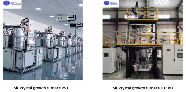
SiC crystal growth furnace PVT/HTCVD method:

ZMSH's SiC crystal growth furnace PVT/HTCVD:
Q&A
1. Q: What are the key advantages of silicon carbide (SiC) seed crystal wafers?
A: Silicon carbide seed crystal wafers offer extremely high thermal conductivity (4.9 W/cm·K), exceptional breakdown field strength (2–4 MV/cm), and a wide bandgap (3.2 eV), enabling stable performance in high-temperature, high-voltage, and high-frequency applications like power electronics and RF devices .
2.Q: What industries use SiC seed crystal wafers?
A: They are critical for semiconductors (MOSFETs, diodes), renewables (solar inverters), automotive (EV inverters), and aerospace (radiation-resistant electronics), enhancing efficiency and reliability in extreme conditions.
Tag: #SiC crystal seed wafers, #Shape and size customized, #4H-N type, #Dia 153,155, 205, 203, 208, # 2inch-12inch, #manufacturing MOSFETs, #Production Grade, #PVT/HTCVD growth
Get in Touch
Have questions about our products or want to discuss a custom order? Our team is ready to help you.