
HPSI High Purity Semi-insulating SiC Wafers 2"3"4"6" 8" Prime/Dummy/Research Grade
HPSI High Purity Semi-insulating SiC Wafers – 2/3/4/6/8 Inch Prime/Dummy/Research Grade
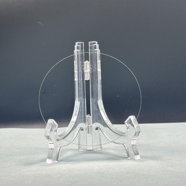
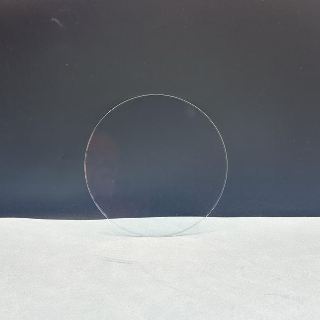
HPSI (High Purity Semi-insulating) Silicon Carbide (SiC) wafers are advanced semiconductor substrates designed for high-frequency, high-power, and high-temperature applications. Available in 2-inch, 3-inch, 4-inch, 6-inch, and 8-inch diameters, these wafers are offered in Prime (production-grade), Dummy (process-testing), and Research (experimental) grades to meet diverse industrial and academic needs.
The Prime Grade wafers feature ultra-low defect density and high resistivity, making them ideal for RF devices, power amplifiers, and quantum computing applications. The Dummy Grade provides cost-effective solutions for process optimization in semiconductor fabrication, while the Research Grade supports cutting-edge material studies and prototype development.
With superior thermal conductivity (> 490 W/m·K) and a wide bandgap (3.2 eV), HPSI SiC wafers enable next-generation electronics for 5G communications, aerospace, and electric vehicle (EV) systems.
Specifications Table
| Propertise | Specification |
| Type | 4H-Semi |
| Resistivity | ≥1E8ohm·cm |
| Thickness | 500±25μm |
| On-axis | <0001> |
| Off-axis | 0±0.25° |
| TTV | ≤5μm |
| BOW | -25μm~25μm |
| Wrap | ≤35μm |
| Front (Si-face) Roughness | Ra≤0.2nm(5μm*5μm) |
Applications of HPSI Wafers
1. RF & Microwave Devices
- 5G Base Stations: High-power amplifiers with low signal loss.
- Radar Systems: Stable performance in aerospace and defense.
2. Power Electronics
- EV Inverters: Efficient high-voltage switching.
- Fast Chargers: Compact and high-efficiency designs.
3. High-Tech Research
- Wide-Bandgap Studies: Research on SiC material properties.
4. Industrial Process Development
- Dummy Wafers: Equipment calibration in semiconductor fabs.
Frequently Asked Questions (FAQ)
1. What defines "Semi-insulating" SiC?
Semi-insulating SiC has extremely high resistivity, minimizing current leakage in RF and high-power devices.
2. Can these wafers be customized?
Yes, we offer doping, thickness, and surface finish customization for Prime and Research grades.
3. What is the difference between Prime and Dummy grades?
- Prime: Device fabrication (low defects).
- Dummy: Process testing (cost-optimized).
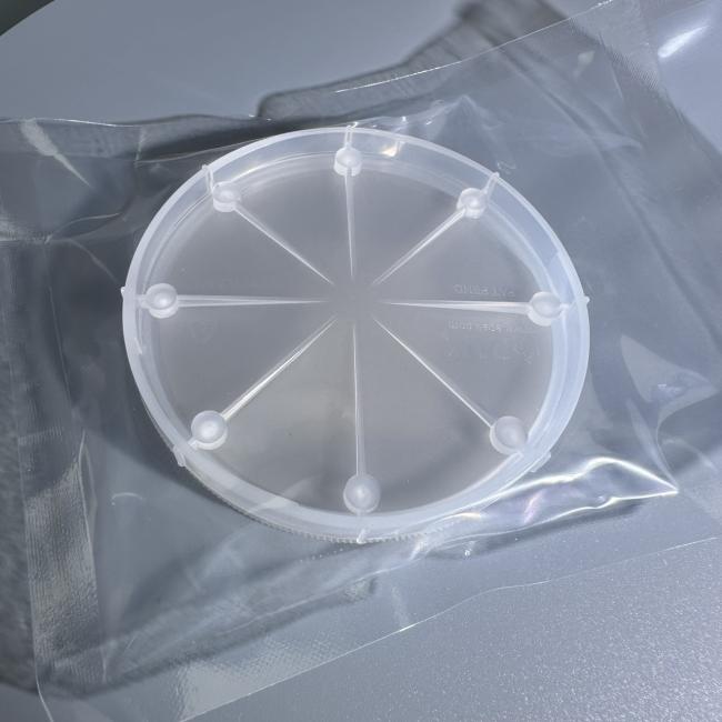
4. How are wafers packaged?
Single-wafer vacuum-sealed packs
5.What is the typical lead time?
- 2-4 weeks for standard sizes.
- 4-6 weeks for custom specifications.
Tags: #HPSI, #High Purity, #Semi-insulating, #SiC Wafers, #2",3",4",6", 8", #Prime/Dummy/Research Grade, #AR Glasses, #Optical Grade
Get in Touch
Have questions about our products or want to discuss a custom order? Our team is ready to help you.