
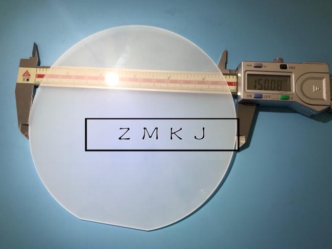
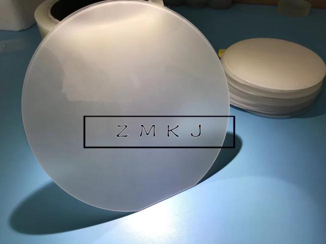
Sapphire Wafer 6'' Dia 150mm±0.1mm Thickness 1000um C-Plane
Sapphire Wafer 6" Dia 150mm±0.1mm Thickness 1000um C-plane 99.99%pure
Our 6-inch diameter sapphire wafers are precision-engineered single crystal Al₂O₃ substrates designed for demanding semiconductor applications. With strict diameter control at 150.0±0.1mm and standard thickness of 1000±15μm, these C-plane (0001) oriented wafers deliver exceptional performance for:
- GaN-based LED and power device production
- High-frequency RF components
- Advanced optical systems
Specifications
|
Parameter |
Specification |
|---|---|
| Diameter | 150.0 ±0.1 mm |
| Thickness | 1000 ±10 μm |
| Orientation | (0001) ±0.15° |
| TTV | <10 μm |
| Warp | ≤20 μm |
| Bow | -15um≤BOW≤0 |
| Warp | <10 μm |
Applications of Sapphire Wafers
Sapphire Wafers in Optoelectronics
- Micro-LED displays
- UV sterilization devices
- High-brightness lighting
Sapphire Wafers in Power Electronics
- GaN HEMTs for 5G/6G
- EV power modules
- Radar systems
Sapphire Wafers in Emerging Technologies
- Quantum dot devices
- MEMS resonators
- Photonic sensors
KEY Features of Sapphire Wafer
1. Sapphire Wafers's Superior Thermal Performance
- High thermal conductivity: 35 W/m·K @25°C
- Low CTE: 5.3×10⁻⁶/K (25-500°C)
- Thermal shock resistant: Withstands ΔT >500°C
2. Sapphire Wafers's Optical Excellence
- Broadband transmission: 85%@250nm → 92%@450nm → 90%@4000nm
- Minimal birefringence: <3 nm/cm @633nm
- Laser-grade polish: PV <λ/4 @633nm
3. Sapphire Wafers's Mechanical Robustness
- Extreme hardness: 2000 HV (Mohs 9)
- High flexural strength: 700±50 MPa
- Young's modulus: 400 GPa
4. Sapphire Wafers's Manufacturing Advantages
- Diameter control: 150.0±0.1mm (compatible with 6" tools)
- Thickness options: 430-1000μm available
- Edge profiling: Notched or laser-marked per SEMI standards
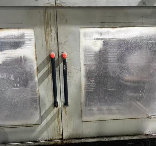
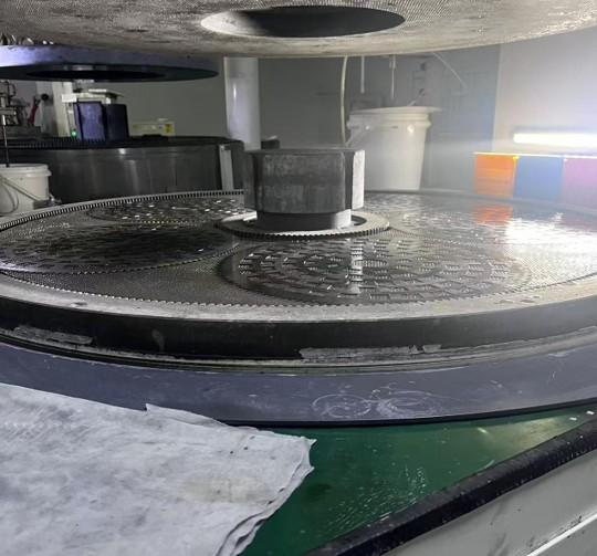
Sapphire Wafer manufacture process
1. Orientation: Accurately locate the sapphire crystal rod position on the slicing machine, so as to facilitate precise slicing processing

2. Slicing: Cut the sapphire crystal rod into thin wafers
3. Grinding: Remove the chip cutting damage layer caused by slicing and improve the flatness of the wafer
4. Chamfering: Trim the wafer edge into a circular arc to improve the mechanical strength of the wafer edge to avoid the defects caused by stress concentration
5. Polishing: Improve the roughness of the wafer to reach the epitaxial wafer's precision
6. Cleaning: Remove the contaminants on the wafer surface (such as dust particles, metals, organic contaminants)
7. Quality inspection: The wafer's quality (flatness, surface dust particles, etc.) shall be inspected with high-precision testing instruments to meet customer requirements
Get in Touch
Have questions about our products or want to discuss a custom order? Our team is ready to help you.