
2inch 4inch 6inch 8inch 5×5 mm 10×10 mm 4H-SiC Substrates 3C-N Type MOS Grade
Overview of 3C-SiC Substrates
2inch 4inch 6inch 8inch 5×5 mm 10×10 mm 4H-SiC Substrates 3C-N Type MOS Grade
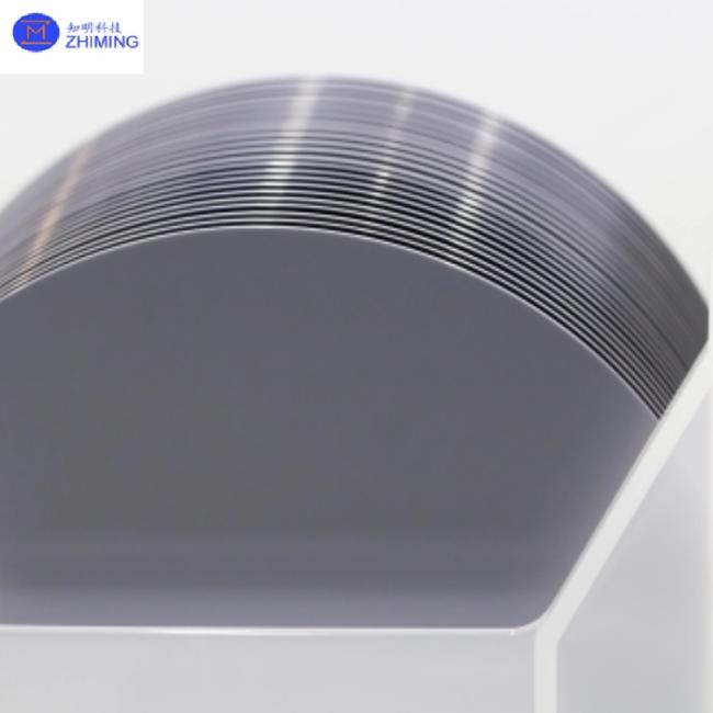
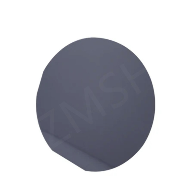
3C-N type silicon carbide (3C-SiC) substrate is a wide-bandgap semiconductor material based on the cubic crystal structure (3C), fabricated via liquid phase epitaxy (LPE) or physical vapor transport (PVT). It supports standard sizes from 2-inch to 8-inch, as well as custom dimensions (e.g., 5×5 mm, 10×10 mm). Its core advantages include high electron mobility (1,100 cm²/V·s), wide bandgap (3.2 eV), and high thermal conductivity (49 W/m·K), making it ideal for high-frequency, high-temperature, and high-power device applications.
Key Characteristics of 3C-SiC Substrates

1. Electrical Performance
- High Electron Mobility: Significantly superior to 4H-SiC (900 cm²/V·s), 3C-SiC substrates reducing conduction losses in devices.
- Low Resistivity: ≤0.0006 Ω·cm (N-type), 3C-SiC substrates optimized for low-loss high-frequency circuits.
- Wide Bandgap: Withstands voltages up to 10 kV, 3C-SiC substrates suitable for high-voltage scenarios (e.g., smart grids, EVs).
2. Thermal & Chemical Stability
- High Thermal Conductivity: 3× higher heat dissipation efficiency than silicon, 3C-SiC substrates operating stably from -200°C to 1,600°C.
- Radiation Resistance: 3C-SiC substrates ideal for aerospace and nuclear applications.
3. Process Compatibility
- Surface Flatness: λ/10 @632.8 nm, compatible with lithography and dry etching.
- Low Defect Density: Micro-tube density <0.1 cm⁻², enhancing device yield.
Core Applications of 3C-SiC Substrates
1. 5G Communications & RF Devices
- Millimeter-Wave RF Modules: 3C-SiC substrates enables GaN-on-3C-SiC RF devices for 28 GHz+ bands, improving signal efficiency.
- Low-Loss Filters: 3C-SiC substrates reduces signal attenuation, boosting radar and communication sensitivity.
2. Electric Vehicles (EVs)
- On-Board Chargers (OBC): 3C-SiC substrates reduces energy loss by 40%, compatible with 800V fast-charging platforms.
- Inverters: 3C-SiC substrates cuts 80–90% energy loss, extending driving range.
3. Industrial & Energy Systems
- Solar Inverters: Improves conversion efficiency by 1–3%, reducing volume by 40–60% for high-temperature environments.
- Smart Grids: Minimizes heat dissipation needs, supporting high-voltage DC transmission.
4. Aerospace & Defense
- Radiation-Hardened Devices: Replaces silicon components, extending satellite and rocket system lifespans.
- High-Power Radars: 3C-SiC substrates leverages low-loss properties for enhanced detection precision.
3C-SiC Substrates of Material Technical Parameter
| Grade | Zero MPD Production Grade (Z Grade) | Standard Production Grade (P Grade) | Dummy Grade (D Grade) | ||
| Diameter | 145.5 mm–150.0 mm | ||||
| Thickness | 350 μm ±25 μm | ||||
| Wafer Orientation | Off axis: 2.0°-4.0°toward [1120]± 0.5° for 4H/6H-P, On axis: ⟨111⟩ ± 0.5° for 3C-N | ||||
| ** Micropipe Density | 0 cm⁻² | ||||
| ** Resistivity | p-type 4H/6H-P | ≤0.1 Ω·cm | ≤0.3 Ω·cm | ||
| n-type 3C-N | ≤0.8 mΩ·cm | ≤1 mΩ·cm | |||
| Primary Flat Orientation | 4H/6H-P | {1010} ±5.0° | |||
| 3C-N | {110} ±5.0° | ||||
| Primary Flat Length | 32.5 mm ±2.0 mm | ||||
| Secondary Flat Length | 18.0 mm ±2.0 mm | ||||
| Secondary Flat Orientation | Silicon face up, 90° CW. from Prime flat ±5.0° | ||||
| Edge Exclusion | 3 mm | 6 mm | |||
| LTV/TIV/Bow/Warp | ≤2.5 μm/≤5 μm/≤15 μm/≤30 μm | ≤10 μm/≤15 μm/≤25 μm/≤40 μm | |||
| * Roughness | Polish Ra≤1 nm | ||||
| CMP Ra≤0.2 nm | Ra≤0.5 nm | ||||
| Edge Cracks By High Intensity Light | None | Cumulative length≤10 mm, single length≤2 mm | |||
| * Hex Plates By High Intensity Light | Cumulative area≤0.05% | Cumulative area≤0.1% | |||
| * Polytype Areas By High Intensity Light | None | Cumulative area≤3% | |||
| Visual Carbon Inclusions | None | Cumulative area≤0.05% | |||
| # Silicon Surface Scratches By High Intensity Light | None | Cumulative length≤1×wafer diameter | |||
| Edge Chips High By Intensity Light | None permitted≥0.2mm width and depth | 5 allowed, ≤1 mm each | |||
| Silicon Surface Contamination By High Intensity | None | ||||
| Packaging | Multi-wafer Cassette or Single Wafer Container | ||||
Notes:
* Defects limits apply to entire wafer surface except for the edge exclusion area.
* The scratches should be checked on Si face only.
Recommend other models of SiC

Q1: What are the key applications of 2-inch, 4-inch, 6-inch, 8-inch, 5×5mm, and 10×10mm 3C-N-type SiC substrates?
A: They are widely used in 5G RF modules, EV power systems, and high-temperature industrial devices due to their high electron mobility and thermal stability.
Q2: How do 3C-N-type SiC substrates compare to traditional 4H-SiC in performance?
A: 3C-N-type SiC offers lower resistance and better high-frequency performance (up to 2.7×10⁷ cm/s electron velocity), ideal for RF and compact power electronics.
Tag: #Silicon carbide substrate, #3C-N type SIC, #Semiconductor materials, #3C-SiC Substrate, #Product Grade, #5G Communications, #2inch/4inch/6inch/8inch/5×5 mm/10×10 mm, #MOS Grade, #4H-SiC Substrates
Get in Touch
Have questions about our products or want to discuss a custom order? Our team is ready to help you.