
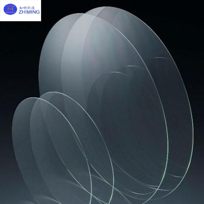
JGS1 JGS2 Wafers Optical Grade Fused Quartz Wafers 2-12 inch
JGS1 JGS2 Wafer Summary
JGS1 JGS2 Wafers Optical Grade Fused Quartz Wafers 2-12 inch
JGS1 and JGS2 are both types of high-purity synthetic quartz glass, primarily composed of silicon dioxide (SiO₂). The fundamental difference between them lies in their manufacturing processes and the resulting purity and optical properties.
•JGS1 is produced using the Chemical Vapor Deposition (CVD) method. It features extremely low metallic impurity content (typically controlled below 0.1 ppm) and very low hydroxyl (OH) content (<5 ppm). This grants it exceptional transmittance in the deep ultraviolet (DUV) spectrum (e.g., over 85% transmittance at 185 nm wavelength for a 10mm thick blank). Furthermore, it has minimal internal bubbles and streaks, offering extremely high optical homogeneity.
•JGS2 is typically produced using the hydrogen-oxygen flame fusion method. It has a relatively higher metallic impurity content (approx. 1 ppm) and a higher hydroxyl content (typically 30-50 ppm). This results in good performance from the ultraviolet (UV) to near-infrared (NIR) spectrum (typically >80% transmittance at 220 nm wavelength), but it exhibits a significant absorption band in the 2600-2800 nm range. Its internal structure may contain minor bubbles, granular structures, or rotational streaks.
In simple terms, JGS1 represents the pursuit of ultimate UV transmittance and ultra-high performance ("high purity"), while JGS2 offers a more cost-effective choice while meeting the needs of most UV and visible light applications.
Quartz Wafer JGS1 JGS2 Key Features
For an intuitive comparison, the core characteristics of JGS1 and JGS2 are summarized in the table below.
| Characteristic Dimension | JGS1 (Far Ultraviolet Optical Quartz Glass) | JGS2 (Ultraviolet Optical Quartz Glass) |
| Optical Transmission Range |
185 nm - 2500 nm
|
220 nm - 2500 nm
|
| Transmittance @185nm/220nm |
>85% @185nm (10mm thick)
|
>80% @220nm (10mm thick)
|
| 2600-2800nm Absorption |
Presence of strong absorption band
|
Presence of strong absorption band
|
| Metallic Impurity Content |
Extremely Low (approx. 0.1 ppm)
|
Relatively Low (approx. 1 ppm)
|
| Hydroxyl (OH) Content |
Very Low (<5 ppm)
|
Higher (30-50 ppm)
|
| Internal Defects |
Very few bubbles and streaks, extremely high optical homogeneity
|
May contain minor bubbles, granular structures, or rotational streaks
|
| Thermal Coefficient of Refractive Index (dn/dT) | Relatively Higher |
Lower (e.g., ~1.2×10⁻⁶/℃ @1550nm), superior thermal stability
|
| Surface Micro-Roughness | Extremely Low (RMS can reach 0.2 nm), suitable for λ/20 machining requirements | High surface hydroxyl density after HF treatment, providing an ideal interface for coating |
| Typical Manufacturing Process |
Chemical Vapor Deposition (CVD)
|
Hydrogen-Oxygen Flame Fusion
|
Beyond the key features in the table above, they also share some excellent common qualities:
•High Heat Resistance: Softening point around 1683°C, can withstand continuous operating temperatures of 1100°C.
•Low Thermal Expansion Coefficient: Approximately 5.15×10⁻⁷/℃ (at 100°C), indicating good thermal stability.
•Good Chemical Stability: Resistant to various acids and alkalis.
•Relatively High Mechanical Strength: Mohs hardness of about 7.
JGS1 JGS2 Quartz wafer Main Applications

Due to their unique properties, JGS1 and JGS2 are used in different high-end fields.
JGS1 Applications (Pursuing Ultimate UV Performance)
Owing to its extremely high UV transmittance and ultra-low impurities, JGS1 is primarily used in:
- Semiconductor Lithography: A key material for optical components (e.g., lenses, mask plates) in Deep Ultraviolet (DUV) lithography systems. Its purity directly affects the linewidth and yield of chip manufacturing.
- High-End UV Laser Systems: Used for manufacturing optical windows and lenses in excimer lasers and UV laser processing equipment, capable of withstanding high-energy laser radiation.
- Precision Optical Detection and Sensing: Used in core optical components of ozone monitoring sensors, UV spectrometers, and other scenarios requiring deep UV transmission.
- Optical Communication Filter Devices: In Dense Wavelength Division Multiplexing (DWDM) systems, its ultra-low loss and excellent spectral stability (transmittance fluctuation <0.1%/nm in the C-band) make it highly suitable for substrates of filters like Arrayed Waveguide Gratings (AWG), allowing channel spacing to be compressed to 50 GHz.

JGS2 Applications (Balancing Performance and Cost)
JGS2's good performance in the UV to NIR region gives it a wide range of applications:
- Fiber Optic Communication: Used for manufacturing optical connectors, optical isolator windows, etc. Its superior thermal stability (lower dn/dT) is valuable for optical mirrors requiring temperature compensation, with reflectivity reaching up to 99.998% at 1550 nm.
- Industrial UV Processing: Used for lamp housings and observation windows in high-pressure mercury lamps and UV sterilization equipment, as well as general UV optical windows.
- General Optical Components: A cost-effective choice for manufacturing conventional optical elements like lenses, prisms, and mirrors, commonly found in optical instruments such as microscopes and telescopes.
- Other Lithography Process Steps: Although not directly used in the most advanced lithography core lenses, it can be used in other steps or equipment requiring UV transmission where ultimate performance is not critical.
Quartz Wafer JGS1 JGS2 Physical Property
| Mechanical Properties | |
| Density/g/cm³ | 2.2 |
| Mohs hardness | 6-7 |
| Compressive Strength | 1100 |
| Tensile Strength | 50 |
| Bending Strength | 65 |
| Torsional Strength | 30 |
| Young's Modulus | 7.5 * 104 GPa |
| Poisson Ratio | 0.17 |
| Electrical Properties | |
| Dielectric Constant (10GHz) | 3.74 |
| Loss Factor (10GHz) | 0.0002 |
| Dielectric Strength (10GHz) | 3.7 * 107 V·m |
| Resistivity (20℃) | 1 * 1020 Ω·m |
| Resistivity (1000℃) | 1 * 108 Ω·m |
| Thermal Properties | |
| Strain Point | 1080 |
| Annealing point | 1180 |
| Softening point | 1630 |
| Thermal Conductivity(20℃) | 1.4 |
| Specific Heat (20 ℃) | 670 |
| (20–320℃)Expansion Coefficient: 30℃–600℃ |
5.5 * 10-7 |
Related product recommendations
1. Through Glass Vi (TGV) JGS1 JGS2 Sapphire BF33 Quartz Customizable Dimensions

2. Quartz Glass Fused Silica Radiation Shielding Windows JGS1/JGS2/JGS3 Transparent UV

Quartz Wafer JGS1 JGS2 FAQ
1. Q: What is the difference between JGS1 and JGS2 fused silica wafers?
A: JGS1 offers superior deep ultraviolet (DUV) transmission due to its extremely low metallic impurities and hydroxyl content, while JGS2 provides cost-effective performance for UV to near-infrared applications but with higher OH content and a significant absorption band at 2600-2800 nm.
2. Q: Which applications are best suited for JGS1 versus JGS2 wafers?
A: JGS1 is ideal for deep UV applications like semiconductor lithography and excimer lasers, whereas JGS2 is commonly used in general UV optics, fiber communications, and industrial UV processing where extreme DUV performance is not critical.
Tags: #JGS1 JGS2 Wafers, #Custom, #Optical Grade, #Fused Quartz Wafers, #2-12 inch
Get in Touch
Have questions about our products or want to discuss a custom order? Our team is ready to help you.