
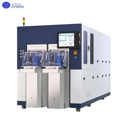
6–8 Inch Silicon and SiC Wafer Polishing Line with Quad Heads and Closed-Loop Mounting
6–8 Inch Silicon and SiC Wafer Polishing Line with Quad Heads and Closed-Loop Mounting
Product Overview
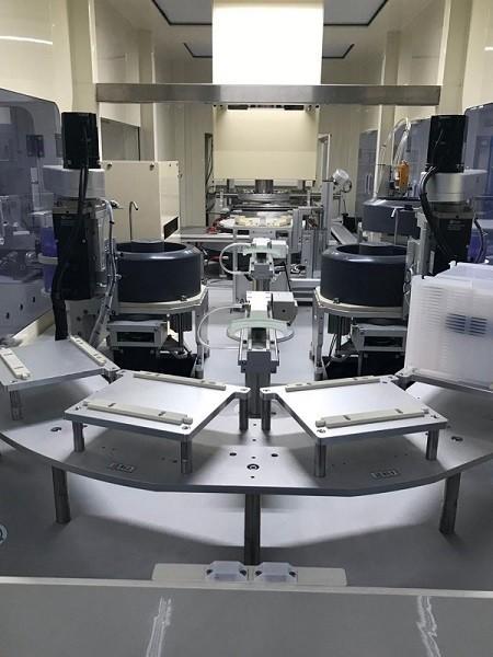
The 6–8 inch Semiconductor Wafer Polishing Automation Line is a fully integrated post-polishing production system designed for silicon and silicon-carbide (SiC) wafers.
It combines quad-head polishing, automatic wafer de-mounting, ceramic carrier management, precision cleaning, and high-accuracy wafer re-mounting into a single closed-loop automation platform.
This system enables continuous, contamination-controlled, high-yield wafer processing, making it ideal for power semiconductor fabs, SiC substrate manufacturers, and advanced packaging wafer lines.
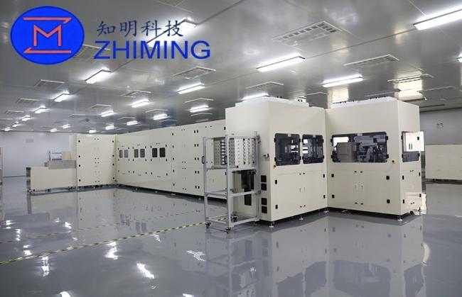
System Architecture
The entire line consists of four highly coordinated process modules:
1. Automatic Wafer De-Mounting Unit
After quad-polishing, wafers are automatically separated from ceramic carriers using low-stress, controlled motion algorithms, preventing:
-
Edge chipping
-
Micro-cracks
-
Residual stress damage
This is especially critical for brittle and high-value SiC wafers.
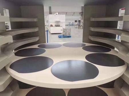
2. Ceramic Carrier Storage & Buffer System
Ceramic carriers are automatically sorted, stored, and dispatched.
The buffer system allows:
-
Continuous operation of the polishing line
-
Multi-spec carrier compatibility
-
Stable takt time control
This eliminates production interruptions caused by manual handling or carrier shortage.
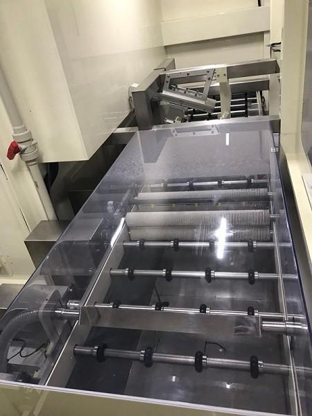
3. Ultra-Clean Ceramic Carrier Washing System
Before re-mounting, each ceramic carrier undergoes deep-level precision cleaning to remove:
-
Polishing slurry
-
Sub-micron particles
-
Chemical residues
This ensures a repeatable, contamination-free surface for every new wafer mounting cycle.
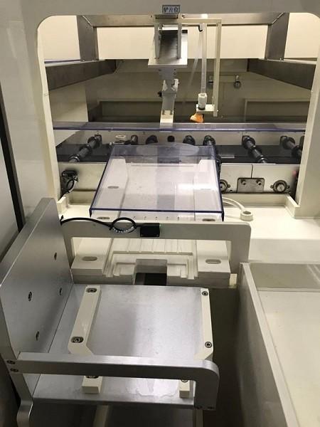
4. High-Precision Wafer Re-Mounting Unit
Wafers are mounted onto cleaned carriers with:
-
Controlled pressure
-
Sub-micron alignment
-
Ultra-high flatness control
This provides the ideal initial condition for the next quad-polishing step, directly improving polishing uniformity and final wafer quality.
Key Process Advantages
Ultra-High Cleanliness
Mounting area cleanliness:
-
≥ 0.5 µm particles: < 50 ea
-
≥ 5 µm particles: < 1 ea
Fully compliant with advanced power semiconductor and SiC manufacturing standards.
Exceptional Mounting Flatness
Mounting flatness ≤ 2 µm
This ensures:
-
Uniform polishing pressure
-
Stable material removal rates
-
Superior thickness uniformity
Critical for high-performance power devices and advanced packaging wafers.
Flexible High-Throughput Production
| Wafer Size | Carrier Diameter | Wafers per Carrier | Cycle Time |
|---|---|---|---|
| 6 inch | 485 mm | 6 wafers | 3 min / carrier |
| 6 inch | 576 mm | 8 wafers | 4 min / carrier |
| 8 inch | 485 mm | 3 wafers | 2 min / carrier |
| 8 inch | 576 mm | 5 wafers | 3 min / carrier |
The system allows manufacturers to balance throughput, cost, and surface quality based on their production strategy.
Technical Specifications
-
Wafer Size: 6–8 inch Silicon & SiC wafers
-
Equipment Dimensions: 13,643 × 5,030 × 2,300 mm (L × W × H)
-
Power Supply: AC 380 V, 50 Hz
-
Total Power Consumption: Approx. 119 kW
-
Mounting Flatness: ≤ 2 µm
-
Mounting Cleanliness:
≥0.5 µm < 50 ea, ≥5 µm < 1 ea
Application
-
Si and SiC power semiconductor wafers (MOSFET, IGBT, diodes)
-
SiC substrates and epitaxial wafers
-
Advanced packaging and interposer wafers
-
Precision device-grade polished wafers
After-Sales Service & Support
-
24/7 remote and on-site technical support
-
Response within 2 hours
-
On-site arrival: within 24 hours (local) / 36 hours (non-local)
-
Free warranty repair and service
-
Lifetime maintenance and spare-parts support
-
Critical spare parts always in stock
-
Regular preventive maintenance visits by field engineers
FAQ – Frequently Asked Questions
Q1: Is this line suitable for both silicon and SiC wafers?
Yes. The system is specifically optimized for both silicon and silicon-carbide wafers. Motion profiles, mounting pressure, and de-mounting trajectories are tuned to handle the high hardness and brittleness of SiC safely.
Q2: How does this system improve polishing yield?
By combining ultra-clean carriers, high flatness mounting, and fully automated handling, the system minimizes:
-
Particle contamination
-
Wafer warpage
-
Pressure non-uniformity
This leads to more stable polishing, lower breakage rates, and higher wafer yield.
Q3: Can the system run continuously with the quad-polisher?
Yes. The carrier buffer and automated logistics are designed to allow 24/7 continuous operation, keeping the quad-polisher running without waiting for manual loading or cleaning.
Related Products
Wafer Thinning System Precision Thinning Equipment SiC Si Wafer Compatible 4 -12inch Wafer Capacity
Get in Touch
Have questions about our products or want to discuss a custom order? Our team is ready to help you.