
8-Inch to 12-Inch Borosilicate and Fused Silica Glass Wafers for Semiconductor and MEMS Applications
8-Inch to 12-Inch Glass Wafer | Borosilicate Glass Wafer and Fused Silica / Fused Quartz Wafer
Our 8-inch to 12-inch glass wafers are high-quality wafer materials designed for semiconductor, MEMS, optical, microfluidic, sensor, display, and research applications. We provide different glass wafer materials, including borosilicate glass wafers and fused silica / fused quartz wafers, to meet various requirements for thermal stability, optical transmission, chemical resistance, dielectric performance, and surface quality.
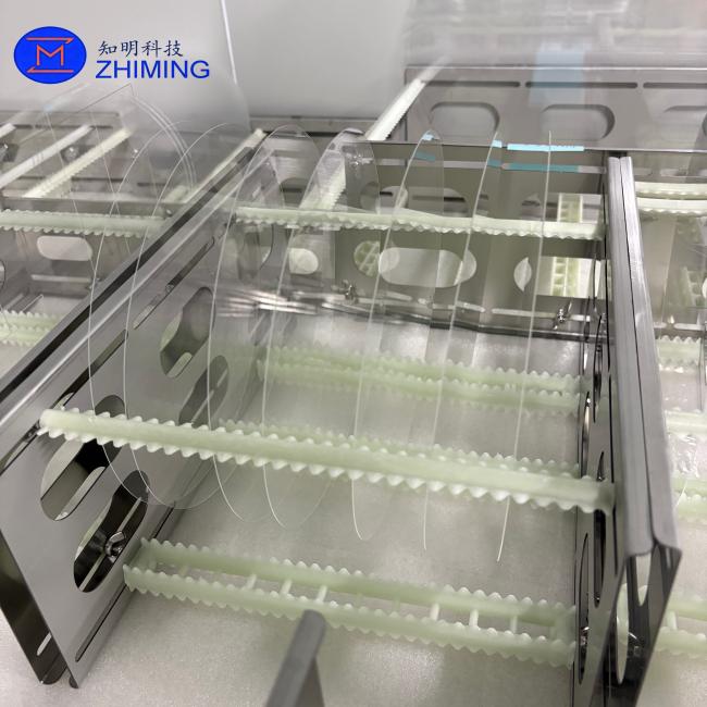
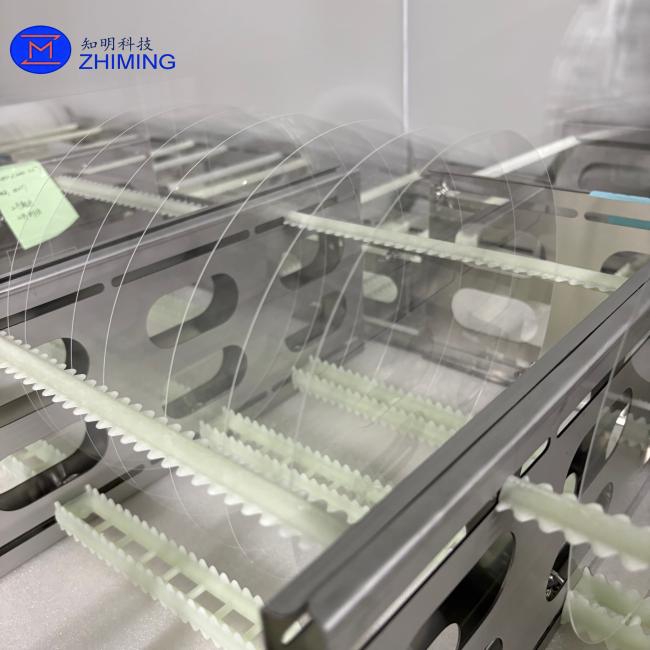
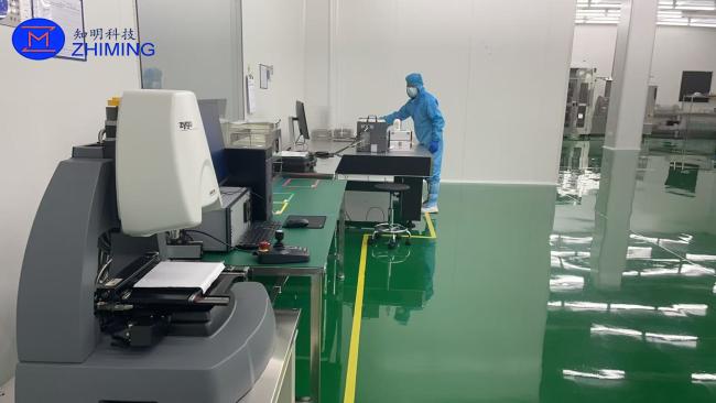
With precise wafer processing, polishing, cleaning, and inspection capabilities, our glass wafers can be customized according to customer requirements, including diameter, thickness, surface finish, TTV, flatness, edge processing, and special specifications.
Product Overview
Glass wafers are widely used as carrier wafers, substrate materials, optical windows, bonding substrates, MEMS substrates, and insulating wafers in advanced manufacturing and research fields.
Compared with silicon wafers, glass wafers offer excellent electrical insulation, optical transparency, chemical stability, and customizable thermal expansion properties. They are especially suitable for applications requiring transparent substrates, low dielectric loss, high surface flatness, or wafer-level bonding compatibility.
We supply glass wafers from 8 inch to 12 inch, including:
- 8-inch glass wafers
- 10-inch glass wafers
- 12-inch glass wafers
- Customized large-size glass wafers upon request
Available Materials
Borosilicate Glass Wafer
Borosilicate glass wafers are commonly used in MEMS, sensors, microfluidic chips, wafer bonding, carrier wafers, and electronic applications. They provide good thermal shock resistance, chemical durability, mechanical stability, and process compatibility.
Borosilicate glass is a practical choice for customers who need a cost-effective glass substrate with stable performance and good dimensional control.
Typical applications include:
- MEMS substrates
- Anodic bonding substrates
- Sensor substrates
- Microfluidic chips
- Wafer-level packaging
- Temporary carrier wafers
- Optical and laboratory substrates
Fused Silica / Fused Quartz Wafer
Fused silica and fused quartz wafers are high-purity glass wafers with excellent optical transmission, low thermal expansion, high temperature resistance, and strong chemical stability.
They are especially suitable for optical, UV, semiconductor, photonics, and high-precision applications where low impurity content, high transparency, and excellent thermal stability are required.
Typical applications include:
- Optical windows
- UV transmission substrates
- Photonics and laser components
- Semiconductor process carriers
- High-temperature insulating substrates
- Precision optical substrates
- Research and laboratory applications
Key Features
- Available in 8-inch to 12-inch wafer sizes
- Borosilicate glass and fused silica / fused quartz options
- Excellent electrical insulation
- Good chemical resistance
- High surface flatness and smoothness
- Optical transparency available depending on material
- Custom thickness and tolerance available
- SSP and DSP surface finish options
- Suitable for semiconductor, MEMS, optical, and research applications
Customizable Specifications
We can provide customized glass wafers according to your project requirements.
Common customizable parameters include:
- Material: Borosilicate glass, fused silica, fused quartz
- Diameter: 8 inch, 10 inch, 12 inch, or customized
- Thickness: Customized
- Surface finish: Single-side polished or double-side polished
- Surface roughness: Available upon request
- TTV: Customized according to application
- Bow and warp: Available upon request
- Edge processing: Chamfered edge, beveled edge, or polished edge
- Holes, slots, or special shapes: Available upon request
- Cleaning and packing: Standard packing or cleanroom packing
If you have drawings, technical specifications, or target applications, our team can help evaluate the most suitable glass wafer solution for your project.
Typical Applications
Our 8-inch to 12-inch glass wafers are suitable for a wide range of advanced manufacturing and research applications, including:
- Semiconductor processing
- MEMS devices
- Wafer-level packaging
- Temporary bonding and carrier wafers
- Microfluidic chips
- Optical windows and substrates
- Sensors
- Photonics
- Display technology
- Laboratory research
- Thin film deposition
- Wafer bonding
Why Choose Our Glass Wafers?
We focus on supplying reliable wafer materials and customized substrate solutions for global customers. Our glass wafers are processed with strict control of thickness, flatness, surface quality, and cleanliness to support demanding applications in semiconductor, optical, and advanced manufacturing fields.
Whether you need borosilicate glass wafers for MEMS and bonding applications, or fused silica / fused quartz wafers for optical and high-temperature applications, we can provide flexible customization and professional technical support.
FAQ
1.Q: What are the main types of glass used?
A: Borosilicate (e.g., Borofloat): Highly affordable, mechanically robust, and provides excellent thermal stability.
Quartz / Fused Silica: Extremely resistant to thermal shock, chemically inert, and offers excellent optical transmission.
2.Q: Why are glass wafers preferred over silicon?
A: Optical Transparency: Allows for through-glass laser debonding and integration with optical sensors.
Electrical Insulation: Glass is an excellent natural dielectric, preventing electrical cross-talk in dense integrated circuits.
Matched Thermal Expansion: Can be engineered to match the Coefficient of Thermal Expansion (CTE) of silicon, enabling strong anodic bonding.
3. Q: What are their key applications?
A: Wafer-Level Packaging & Carriers: Act as temporary or permanent substrates to support ultra-thin silicon wafers during fan-out and 3D IC packaging.
MEMS: Used as transparent protective windows and hermetic caps for sensors (e.g., pressure and acceleration sensors).
Microfluidics: Used to build lab-on-a-chip diagnostic tools due to their high optical clarity and chemical resistance.
Get in Touch
Have questions about our products or want to discuss a custom order? Our team is ready to help you.