
TP1020 Double-Sided PCB with 6.0mm Thickness and ENIG Finish: A High-Performance Solution for RF and Microwave Applications by Bicheng Technologies Limited
TP1020 Double-Sided PCB with 6.0mm Thickness: A High-Performance Solution for RF and Microwave Applications by Bicheng Technologies Limited
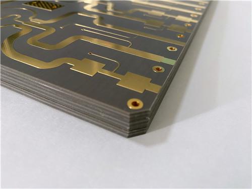
(All PCBs are custom-manufactured. Reference images and parameters may vary based on your design requirements.)
At Bicheng Technologies Limited, we proudly introduce the TP1020 Double-Sided PCB, an innovative high-frequency PCB solution designed for advanced RF and microwave applications. Built with TP1020 thermoplastic laminates, this PCB delivers exceptional dielectric performance, low dissipation factor, and high reliability, making it ideal for satellite navigation systems, missile-borne electronics, and miniaturized antennas.
This 6.0mm thick PCB, featuring a 1oz copper finish, ENIG surface finish, and rigid construction, is tailored for applications requiring stable dielectric properties and minimal signal loss at high frequencies. Let’s explore the construction, features, and applications of this cutting-edge PCB.
1. Overview of the TP1020 Double-Sided PCB
The TP1020 Double-Sided PCB is engineered for high-frequency circuits that demand stable performance, low signal loss, and excellent thermal conductivity. TP1020 thermoplastic laminates are ceramic-filled PPO (polyphenylene oxide) materials, offering adjustable dielectric constants and smooth surfaces for precise and efficient RF designs.
The laminate, free of fiberglass reinforcement, ensures uniform dielectric performance and low moisture absorption, making it ideal for extreme environments and mission-critical applications. At Bicheng Technologies Limited, we guarantee IPC-Class-2 quality standards with 100% electrical testing for every PCB we manufacture.
PCB Construction Details
| Parameter | Specification |
| Base Material | TP1020 |
| Layer Count | 2 layers |
| Board Dimensions | 129mm x 129mm |
| Minimum Trace/Space | 5/8 mils |
| Minimum Hole Size | 0.7mm |
| Blind Vias | No |
| Finished Board Thickness | 6.0mm |
| Finished Copper Weight | 1oz (1.4 mils) outer layers |
| Via Plating Thickness | 20 μm |
| Surface Finish | Electroless Nickel Immersion Gold (ENIG) |
| Top Silkscreen | No |
| Bottom Silkscreen | No |
| Top Solder Mask | No |
| Bottom Solder Mask | No |
| Electrical Testing | 100% tested prior to shipment |
The 2-layer stackup, with TP1020 core material, ensures low signal loss, thermal stability, and mechanical reliability, making this PCB an excellent choice for high-frequency applications.
2. Features and Benefits of TP1020 Material
The TP1020 laminate, part of the TP series, is a premium ceramic-filled thermoplastic material designed for high-frequency and RF applications. With its unique composition, it delivers stable dielectric properties, low dissipation factor, and superior thermal conductivity, even in extreme environments.
Key Features of TP1020:
- Dielectric Constant (Dk): 10.2 ± 0.2 at 10 GHz, ensuring stable and accurate signal propagation.
- Dissipation Factor (Df): 0.0012 at 10 GHz, minimizing energy loss and maintaining circuit efficiency.
- Thermal Properties: Thermal Conductivity: 0.67 W/mK, enabling efficient heat dissipation.
- CTE (Coefficient of Thermal Expansion):
- X-axis: 40 ppm/°C
- Y-axis: 40 ppm/°C
- Z-axis: 55 ppm/°C, ensuring dimensional stability and reliability.
- Low TCDk: -40 ppm/°C, ensuring stable dielectric performance across a wide temperature range (-55°C to 150°C).
- Moisture Resistance: Ultra-low moisture absorption of 0.01%, ensuring stable performance in humid environments.
- Flammability: UL 94-V0, meeting safety standards for high-reliability applications.
Key Benefits of TP1020:
- Adjustable Dielectric Constant: Dielectric constants ranging from 3 to 25 can be tailored to meet specific circuit requirements.
- Low Dielectric Loss: Maintains performance at frequencies up to 10 GHz and beyond.
- Enhanced Thermal Reliability: Suitable for extreme thermal environments, ensuring reliability in mission-critical designs.
- Dimensional Stability: Ceramic-filled PPO composition ensures precision and robustness in high-frequency applications.
- Cost-Effective Manufacturing: Compatible with standard FR-4 processes, reducing production costs.
3. Applications of the TP1020 Double-Sided PCB
The TP1020 Double-Sided PCB is designed for high-frequency RF and microwave systems that demand precision, reliability, and thermal stability. Its unique material properties make it suitable for a wide range of advanced applications.
Typical Applications:
Global Satellite Navigation Systems
Missile-Borne Electronics
Fuze Technology
Miniaturized Antennas
4. Why Choose Bicheng Technologies Limited?
At Bicheng Technologies Limited, we are committed to delivering innovative PCB solutions for high-performance RF and microwave applications. The TP1020 Double-Sided PCB demonstrates our dedication to precision manufacturing, reliable performance, and customer satisfaction.
Why Partner with Us?
Expertise in RF and Microwave PCBs: We specialize in PCBs for high-frequency applications, ensuring superior performance and reliability.
Uncompromising Quality Standards: All PCBs are manufactured to IPC-Class-2 standards and undergo rigorous 100% electrical testing.
Global Availability: We deliver worldwide, ensuring timely support for your projects.
Customer-Centric Approach: Our team provides tailored solutions to meet your specific requirements.
For technical inquiries or assistance, feel free to contact me, Sally, at sales30@bichengpcb.com. I am happy to help you find the perfect PCB solution for your application.
Get in Touch
Have questions about our products or want to discuss a custom order? Our team is ready to help you.